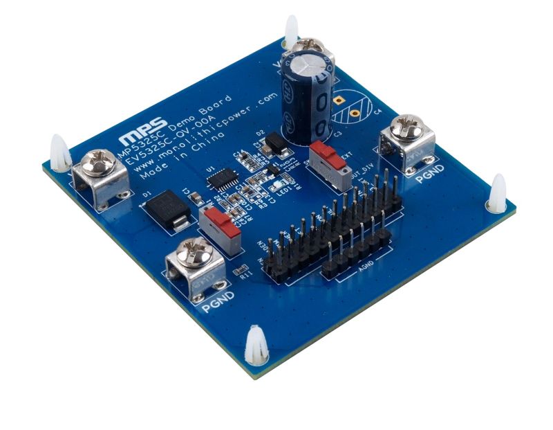
The EV5325C-QV-00A is an evaluation board designed to demonstrate the capabilities of the MP5325C, a fully integrated, hot-swap protection device. The device enables reference circuit evaluation of the MP5325C. It is designed to protect circuitry on its output from transients on its input. It also protects its input from undesired shorts and transients coming from its output. The device can achieve up to 15A of continuous output current (IOUT) per device at room temperature.
During start-up, the inrush current is limited by the slew rate at the output. The slew rate is controlled by an external capacitor (CSS) on the SS pin.
The maximum load at the output is current-limited through the current-sense (CS) MOSFET topology. The magnitude of the current limit is controlled by a low-power resistor connected from the ISET pin to ground.
An internal charge pump drives the power device’s gate, allowing a power MOSFET with a very low 3mΩ on resistance (RDS(ON)) to turn on.
The MP5325C includes an IMON option that produces a voltage proportional to the current flowing through the power device, which is set via a resistor (RIMON) connected between the IMON pin and ground.
Full protection features include current-limiting, thermal shutdown, damaged MOSFET detection, over-voltage lockout (OVLO), and under-voltage lockout (UVLO).
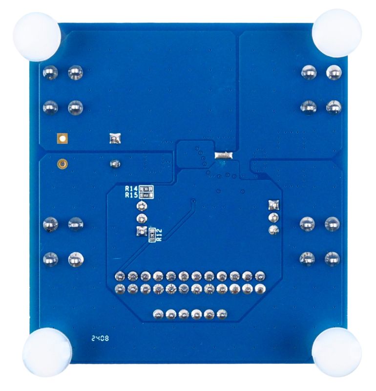
The MP5325C is available in a QFN-22 (3mmx5mm) package. The EV5325C-QV-00A has 4 layers, each of which is 2oz, and the total size is 6.8cmx6.35cm. The MP5325C is included on the board by default.
もっと見る少なく表示
アカウントにログイン
Your email must be verified before you can log in. A message with a link to complete the verification process has been sent to your email address.




 注文
注文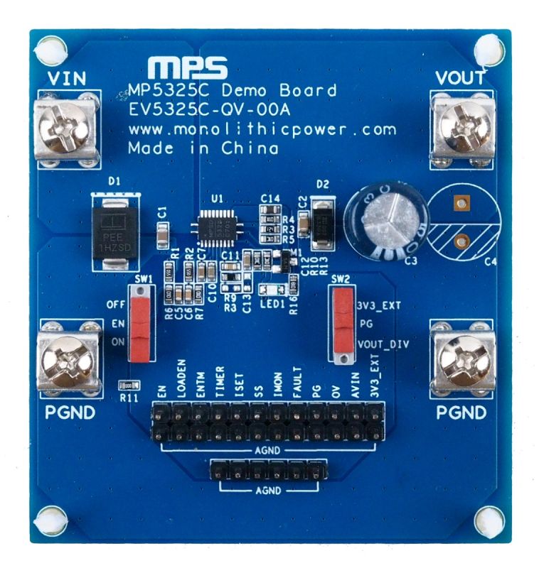






アカウントにログイン
新しいアカウントを作成