Switch-Node Waveform Defines EMC Characteristics for Step-Down Converters in Automotive CISPR 25 Class 5

Get valuable resources straight to your inbox - sent out once per month
We value your privacy
Introduction
Step-down converters’ switch-node voltage waveform defines the electromagnetic compatibility (EMC) behavior for automotive CISPR 25 Class 5 measurements. The ringing frequency in the switch-node waveform is an important signal on the EMC receiver, where a higher ringing amplitude on the switch node often causes EMC issues. Understanding the switch-node waveform enables predicting the converter’s EMC characteristics as well as optimizing EMC filter design at an early design stage.
In this article, an automotive expert compares three MPS automotive step-down converters to provide practical advice on using switch-node waveforms to predict EMC characteristics for automotive CISPR 25 Class 5 measurements. This is helpful to optimize EMC filter design and PCB layout to meet CISPR 25 Class 5 standards.
MPS Automotive Step-Down Converters with Different EMC Characteristics
The MPQ4323M-AEC1 is a 42V, load dump tolerant, ultra-compact, low quiescent current (IQ) synchronous step-down converter with integrated, 100nF, hot-loop multi-layer ceramic capacitors (MLCCs). The internal hot-loop MLCCs reduce the required external filter component count and simplify PCB layout. In addition, these MLCCs achieve excellent EMC properties by significantly reducing ringing in the switch node.
The MPQ4326-AEC1 is a configurable-frequency (200kHz to 2.5MHz), synchronous, step-down switching regulator, which provides up to 6A of highly efficient output current (IOUT) with peak current-mode control. This standard converter is optimized for efficiency and single spread spectrum modulation. Single spread spectrum simplifies passing CISPR 25 Class 5 compared to constant switching frequency (fSW).
The MPQ4371-AEC1 is a synchronous step-down converter with low-noise Quiet-FETTM advanced switching technology that offers a 6A to 11A IOUT range. It also provides dual frequency spread spectrum (FSS) modulation and zero-delay pulse-width modulation (ZDPTM) to achieve fast load step response. This converter optimizes EMC behavior while maintaining high efficiency, and works with dual FSS modulation to further reduce radiated emissions (RE).
Switch-Node Measurements
Switch-node waveforms can be used to compare the EMC characteristics between the MPQ4323M-AEC1, MPQ4326-AEC1, and MPQ4371-AEC1. Figure 1 shows the switch-node measurement on the EVQ4323M-G-00A using an active voltage probe.

Figure 1: Switch-Node Measurement on the EVQ4323M-G-00A Using an Active Voltage Probe
The switch-node voltage waveform typically has a rising time and falling time between 700ps and 2ns. This requires a minimum oscilloscope bandwidth of about 1GHz on the voltage probe tip, where the voltage can be measured with an active probe or a passive probe that has the necessary bandwidth.
For both variants, the ground connection to the PCB must be as short as possible to ensure that the measured ringing on the switch node does not include the additional ringing from the long probe ground connection.
Figure 2 shows the correct voltage probe tip position for the switch-node measurement on the EVQ4323M-G-00A. Connect the GND tip as close as possible to the IC’s PGND pin, and connect the probe input tip as close as possible to the IC’s switch-node pin. Solder the active probe tip with a 0.7pF input capacitance directly to the component pads via removable gold-plated measuring tips.
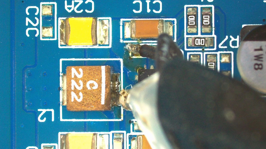
Figure 2: Probe Tip Position for the Switch-Node Measurement on the EVQ4323M-G-00A

Histogram and Time Trend
Figure 3 shows the MPQ4371-AEC1’s switch-node voltage (yellow trace), fSW histogram (pink trace), and time trend (orange trace).
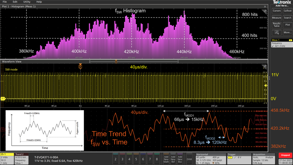
Figure 3: Dual Frequency Spread Spectrum of the MPQ4371-AEC1
The oscilloscope measures the switch-node voltage for each trigger event across a period of 400µs and calculates the frequency of each switching cycle. Each calculated frequency is accumulated in the histogram. The total duration of this test is about 10 minutes. For the last trigger event, the measured frequencies are represented as time trend fSW vs. time.
The measured frequencies in Figure 3 verify the fSW vs. time relationship from the MPQ4371-AEC1 datasheet. The time trend waveform confirms the specified dual frequency spread spectrum modulation frequencies of 15kHz and 120kHz. By verifying proper IC operation, these frequencies provide an overview of the expected fSW values for CISPR 25 Class 5 measurements.
Voltage Waveform
The MPQ4371-AEC1’s switch-node voltage waveform is measured with an active probe. Figure 4 shows the rising and the falling edges of the MPQ4371-AEC1, in which both waveforms are overlaid on the oscilloscope by an alternating rising and falling trigger. The rising edge has a rising time of 922ps and a step response with a 273MHz resonance frequency and a 3.2V peak-to-peak voltage.
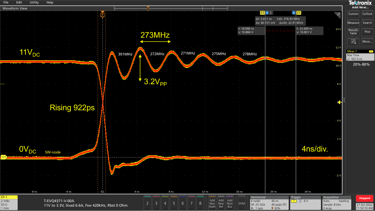
Figure 4: Switch-Node Voltage Waveform for the MPQ4371-AEC1
The MPQ4371-AEC1’s Quiet-FETTM technology enables combining fast slewing edges without excessive ringing. Quiet-FETTM technology does not significantly degrade efficiency like a snubber or bootstrap resistor (RBST), and instead uses a minimum two-step sequential switching action to turn on the internal MOSFETs.
The resonance frequency is determined by the parasitic hot-loop inductances and capacitances. The equivalent hot-loop series inductances (ESL) are defined by the following:
- ESL of the 100nF, 0603-sized MLCC (about 800pH)
- ESL of the high-side MOSFET (HS-FET) and low-side MOSFET (LS-FET)
- ESL of the package lead frame
- ESL of the PCB traces between the MLCC and IC’s VIN and PGND pins (about 700pH/mm)
The switch-node waveform can also be predicted using a simulation of the PCB hot-loop network.
Frequency Domain
Figure 5 shows a fast Fourier transformation (FFT) of the MPQ4371-AEC1’s switch-node waveform. The average fSW of 420kHz is distributed between 384kHz and 456kHz (green markers), and corresponds to the measured histogram from Figure 3. The switch-node resonance frequency at 273MHz is distributed between 250MHz and 300MHz (red markers) due to dual frequency spread spectrum modulation, and corresponds to Figure 4.
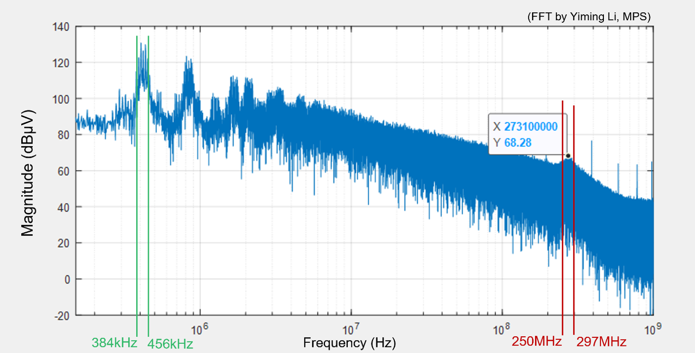
Figure 5: Fast Fourier Transformation of the MPQ4371-AEC1’s Measured Switch-Node Voltage
Radiated Emissions (RE) Antenna for CISPR 25 Class 5
The vertical monopole, biconical, and log periodic antenna measurements in CISPR 25 Class 5 can be analyzed. Figure 6 shows the radiating switching inductance at peak CISPR 25 (blue) and average CISPR 25 (yellow), where the analyzer resolution bandwidth (RBW) = 9kHz, fSW = 420kHz, input voltage (VIN) = 13.5V, output voltage (VOUT) = 3.3V, and load current (ILOAD) = 2.5A. The dual FSS modulation is helpful to maintain RE below the limits.
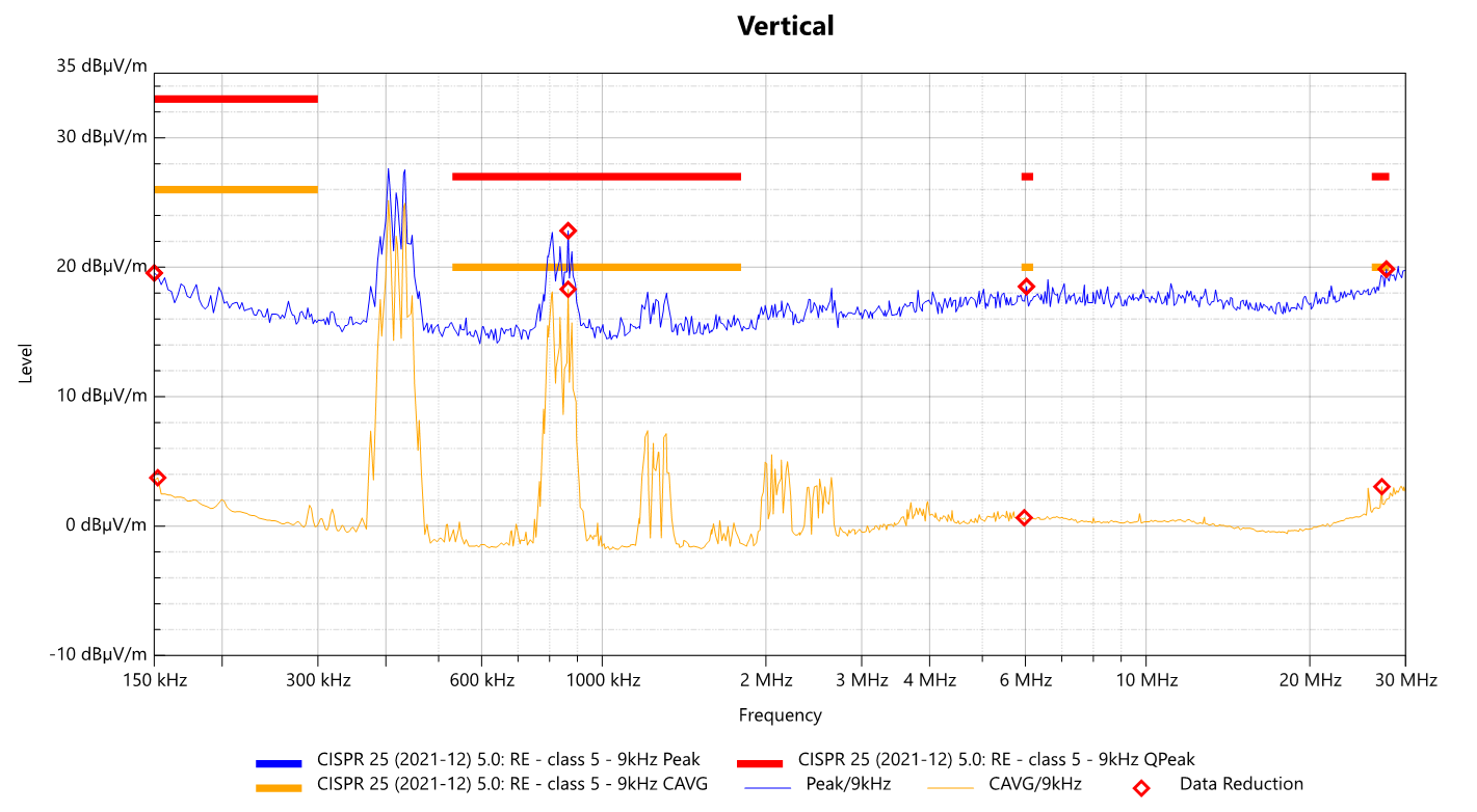
Figure 6: Vertical Monopole Antenna Measurement of the MPQ4371-AEC1 Passes CISPR 25 Class 5
Figure 7 shows the radiating objects (e.g. the harness or radiating traces on the PCB) at peak CISPR 25 (blue) and average CISPR 25 (yellow), where RBW = 120kHz, fSW = 420kHz, VIN = 13.5V, VOUT = 3.3V, and ILOAD = 2.5A.
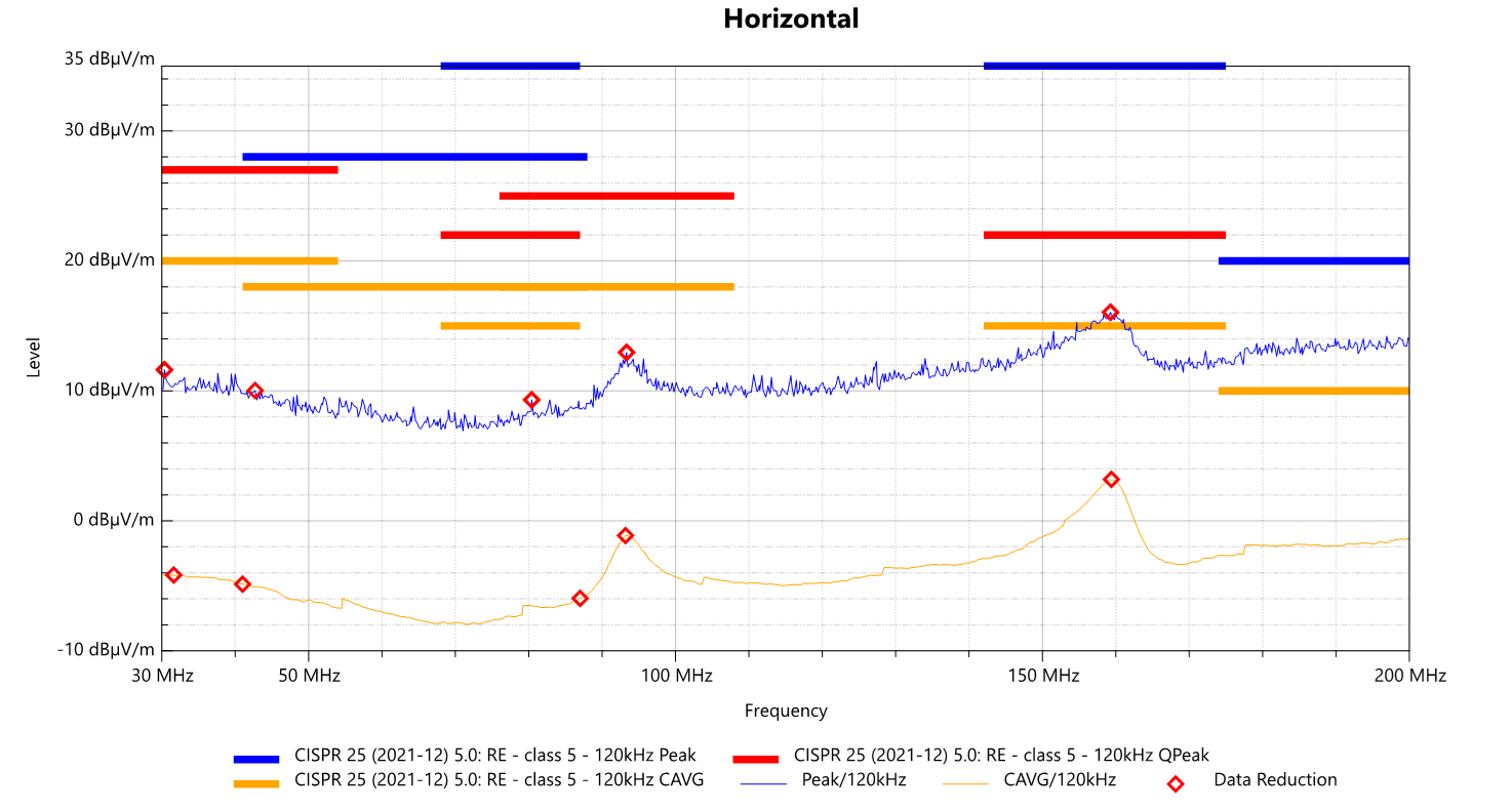
Figure 7: Biconical Antenna Measurement of the MPQ4371-AEC1 Passes CISPR 25 Class 5
Figure 8 shows the switch-node resonance frequencies between 250MHz and 300MHz (corresponding to Figure 4 and Figure 5) at peak CISPR 25 (blue) and average CISPR 25 (yellow), where RBW = 120kHz, fSW = 420kHz, VIN = 13.5V, VOUT = 3.3V, and ILOAD = 2.5A. There is no RE that exceeds the 250MHz to 300MHz resonance frequency range.
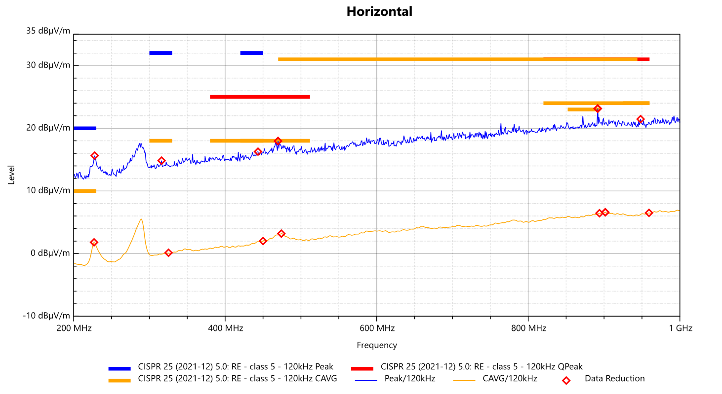
Figure 8: Log Periodic Antenna Measurement of the MPQ4371-AEC1 Passes CISPR 25 Class 5
Figure 9 shows the 1.2GHz switch-node resonance frequency within RE at peak CISPR 25 (blue), average CISPR 25 (yellow), and the noise level (gray), where RBW = 120kHz, fSW = 2.2MHz, VIN = 13.5V, VOUT = 3.3V, and ILOAD = 2.5A.
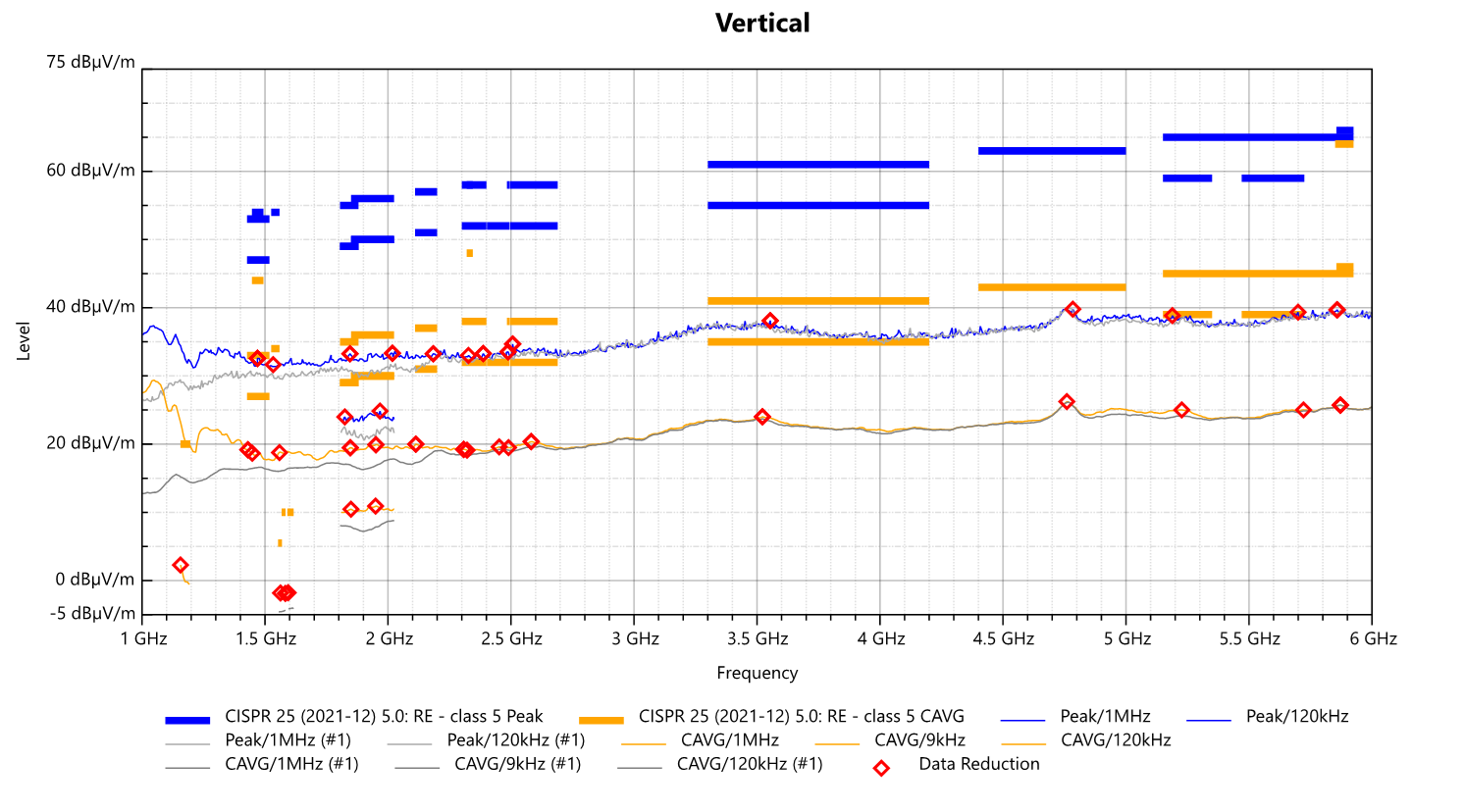
Figure 9: Log Periodic Antenna Measurement of the MPQ4323M-AEC1 Passes CISPR 25 Class 5
Switch-Node Waveform for the MPQ4323M-AEC1
The MPQ4323M-AEC1’s integrated, 100nF, hot-loop MLCCs reduce the internal parasitic inductances, shifts the resonance frequency to higher values, and reduces the resonance amplitude. Figure 10 shows an example of a fast-slewing, state-of-the art switching converter combined with low internal parasitic inductances. This improves the switch-node waveform and reduces RE.
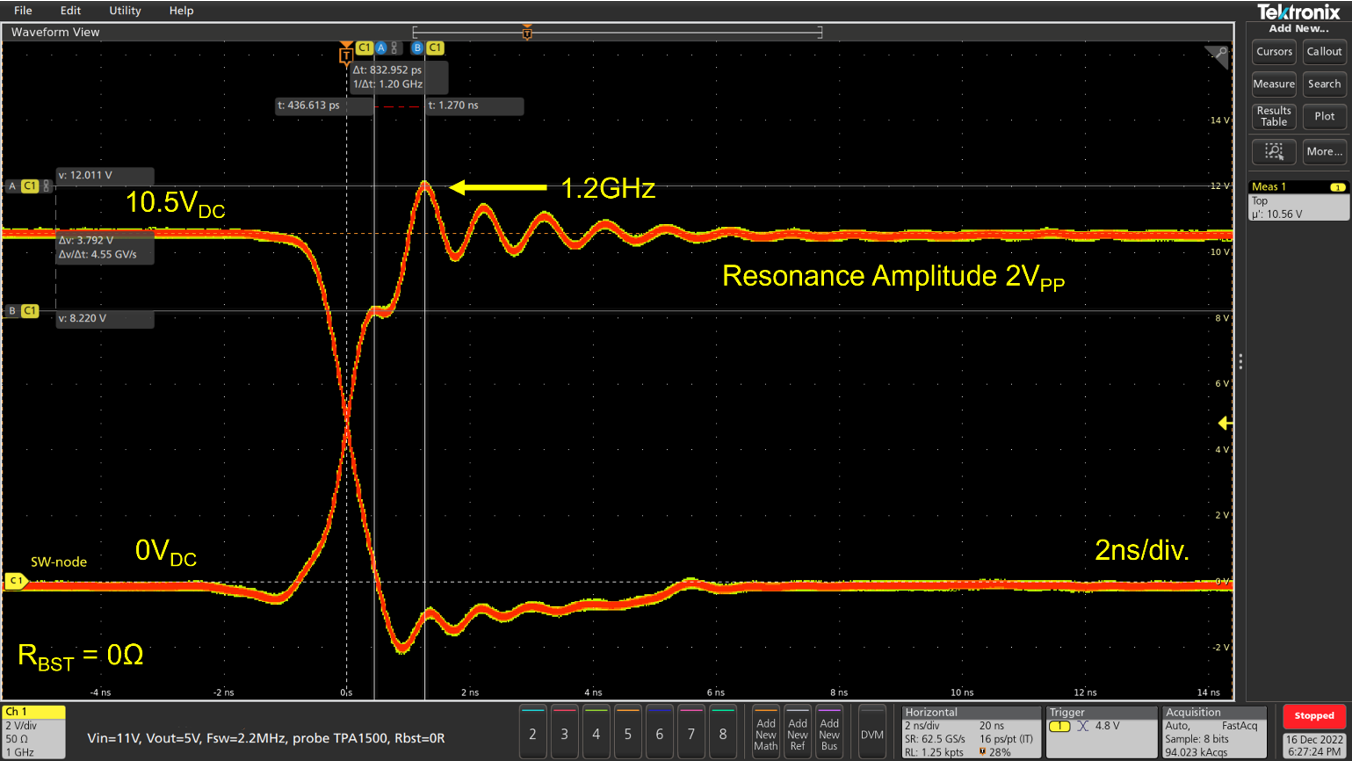
Figure 10: Switch-Node Waveform for the MPQ4323M-AEC1
Switch-Node Example on a 2-Layer PCB
Figure 11 shows two different step-down converters soldered on the same 2-layer PCB. The left curve shows the MPQ4326-AEC1 with frequency spread spectrum modulation on a 2-layer PCB, with a switch-node resonance at 450MHz. The right curve shows a step-down converter in a suboptimal set-up without FSS modulation and a 320MHz resonance. The two converters are compared on the same PCB and with the same external components.
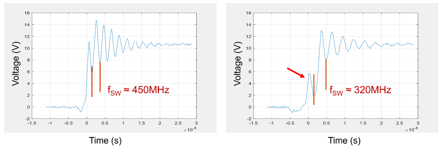
Figure 11: Switch-Node Comparison of Step-Down Converters on a 2-Layer PCB
The step-down converter with the suboptimal set-up indicates undesirable resonance on the rising edge (red arrow), meaning there is a timing difference between the HS-FET and LS-FET. This resonance is caused by using a 2-layer PCB instead of a 4-layer PCB. Compared to a 4-layer PCB, a 2-layer PCB layout has higher parasitic inductances within the hot loop, which increases the resonance amplitude and changes the location of the switch-node resonance. The increased amplitude is observed with both converters. In addition, the 2-layer PCB does not have the important solid ground layer directly under the top layer, resulting in a larger resonance amplitude and stronger RE.
Fast Fourier Transformation (FFT) of Step-Down Converters on a 2-Layer PCB
Figure 12 shows the FFT of the switch-node voltage waveforms for the MPQ4326-AEC1 (with FSS modulation) and step-down converter with the suboptimal set-up (without FSS modulation) from Figure 11.
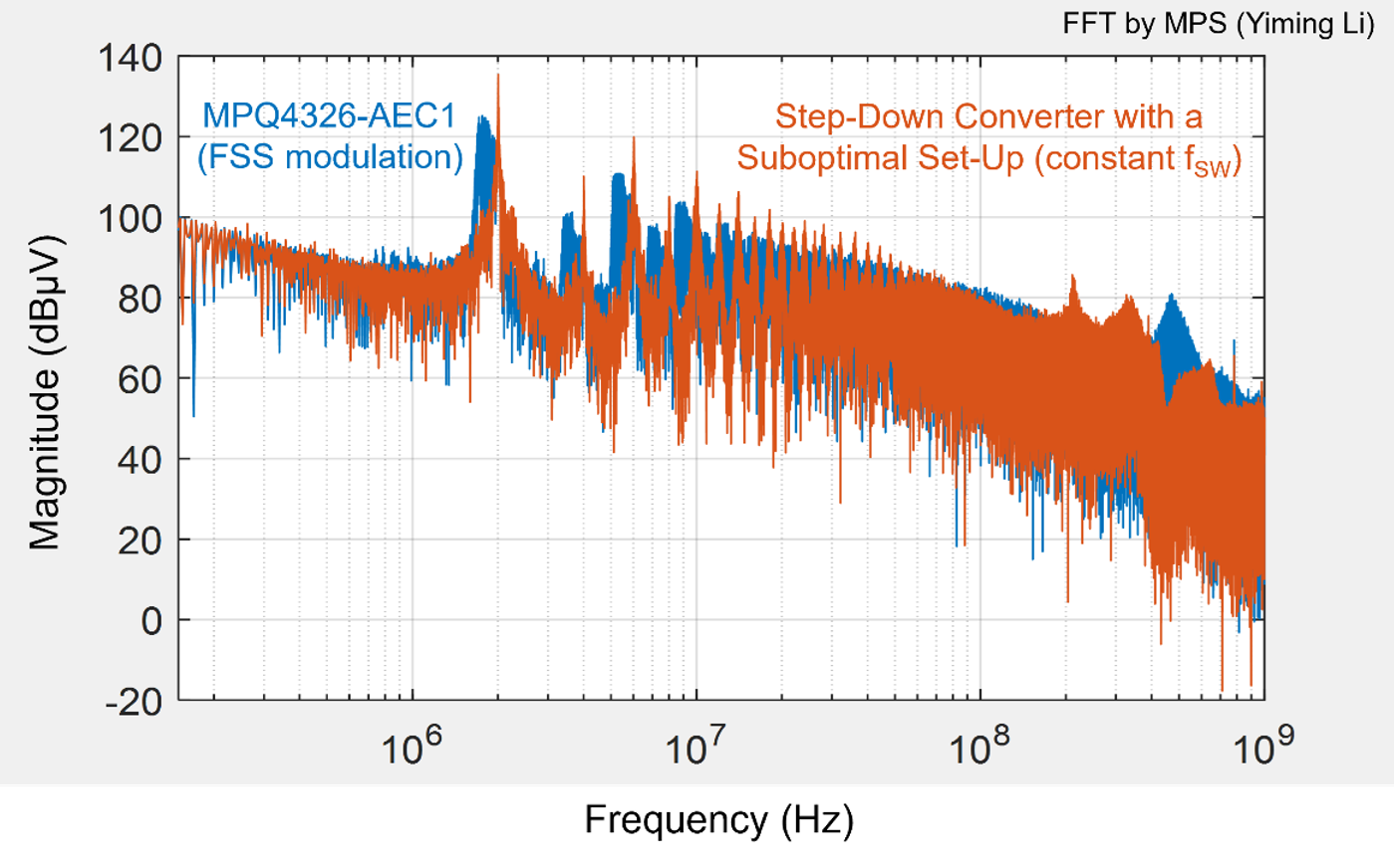
Figure 12: Fast Fourier Transformation of the Switch-Node Voltage Waveforms for the MPQ4326-AEC1 (with FSS Modulation) and Step-Down Converter with a Suboptimal Set-Up (without FSS Modulation)
The MPQ4326-AEC1 uses frequency spread spectrum modulation, while the step-down converter with the suboptimal set-up is set to a constant fSW. Typically, FSS modulation results in lower fundamentals and harmonics. Whether FSS modulation or a constant frequency is more advantageous depends on the requirements of the application. However, FFT shows the differences between the two methods.
The MPQ4326-AEC1’s FFT shows the switch-node resonance at 450MHz, and the step-down converter with the suboptimal set-up shows the switch-node resonance at 320MHz. These switch-node resonance frequencies can be found in the CISPR 25 Class 5 measurements.
Conclusion
This article analyzed the relationship between the switch-node voltage waveform and the frequency domain, using the MPQ4323M-AEC1, MPQ4326-AEC1, and the MPQ4371-AEC1 automotive step-down converters as examples. Understanding the switch-node waveform enables predicting PCB behavior for CISPR 25 Class 5 measurements. The measured resonance frequency shows up in RE measurements, enabling improved EMC filter design for suppressing the resonance frequency. Furthermore, it is possible to assess expected frequency range interferences at an early stage by understanding the switch-node waveform. This helps find a suitable step-down converter according to the application specifications, shorten development times, and reduce costs by simplifying component selection for the EMC filter. To learn more, discover MPS’s robust portfolio of AEC-Q100 qualified switching converters and controllers.
_______________________
Did you find this interesting? Get valuable resources straight to your inbox - sent out once per month!
Technical Forum
 Latest activity 16 hours ago
 1 Comment
Latest activity 2 weeks ago
3 Comments
Latest activity 3 weeks ago
2 Comments
1 Comment
Latest activity 2 weeks ago
3 Comments
Latest activity 3 weeks ago
2 Comments
Log in to your account
Create New Account