


Filtering High-Frequency Interference in Step-Down Converter Designs with Hot-Loop Components
DOWNLOAD PDF


Get valuable resources straight to your inbox - sent out once per month
We value your privacy
Introduction
Modern step-down converters are becoming increasingly efficient. In the frequency range of several hundred MHz, step-down converters can emit higher levels of interference. New IC designs and clever layouts are already able to compensate for such disturbances. By implementing high-frequency ferrite beads, interferences can be further effectively eliminated.
In this article, an automotive expert demonstrates the effectiveness of ferrite beads using an oscilloscope. When placed on the PCB, ferrite beads filter out most of the high-frequency interference, preventing it from radiating through the wiring harness. This is helpful to optimize EMC filter design and PCB layout to meet CISPR 25 Class 5 standards.
Automotive Step-Down Converters with Symmetric VIN Pinout
Symmetric VIN pinout achieves the higher requirements of CISPR 25 Class 5 by using a symmetrical layout arrangement of the hot-loop MLCCs (C1, C2, C3, and C4). The current flowing from the VEMI filter is split symmetrically in the same direction into the IC, cancelling the magnetic field between the two VIN traces. This reduces the overall magnetic field radiated to the environment and allows for effective placement of hot-loop components. (see Figure 1).
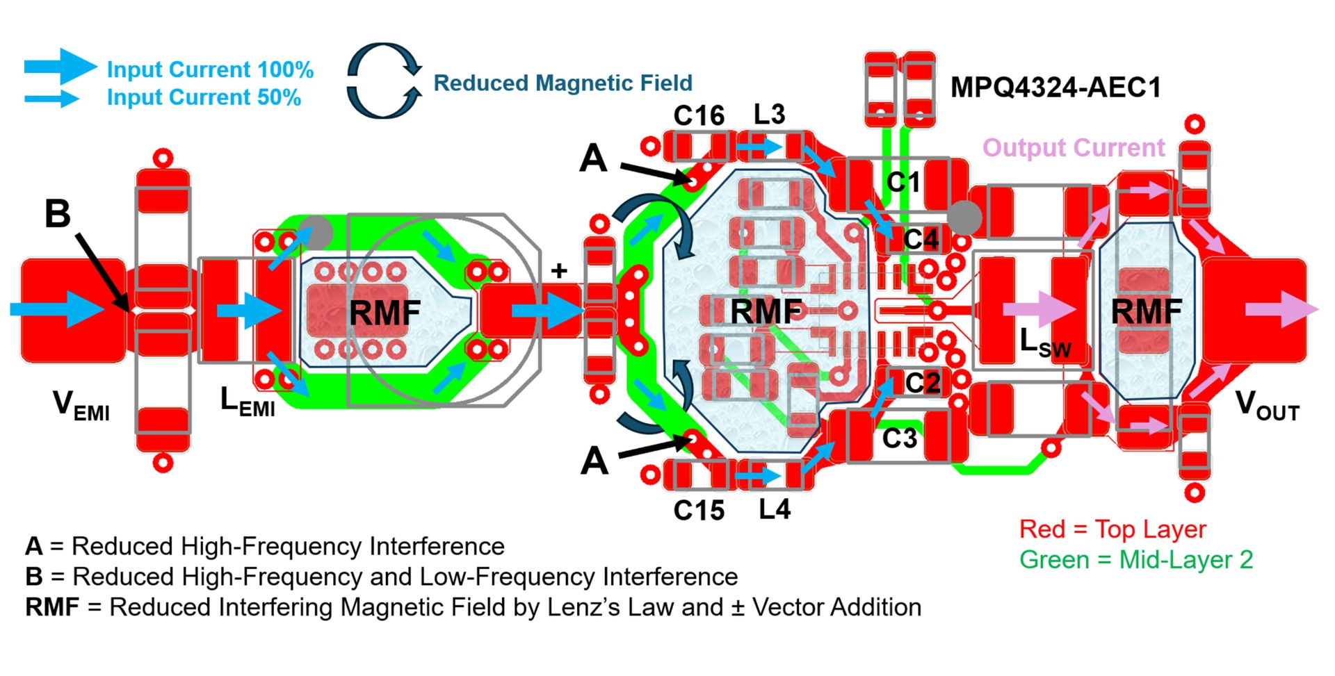
Figure 1: Reduced Magnetic Field Due to Vector Compensation
The MPQ4324-AEC1 is a family of configurable-frequency (350kHz to 2.5MHz), synchronous, step-down switching converters with symmetric VIN pinout, as well as integrated, internal high-side and low-side power MOSFETs (HS-FETs and LS-FETs, respectively). The family provides 0.5A to 3A of continuous output current (IOUT) and 4A of highly efficient peak IOUT with peak current mode control. The MPQ4324-AEC1’s three package variants feature two hot-loop pins for VIN and two hot-loop pins for PGND, which achieve reduced EMI.
Other automotive step-down converters with symmetric VIN pinout include the MPQ4334-AEC1, MPQ4326B-AEC1, MPQ4371-AEC1, and MPQ4385-AEC1, which offer a wide 0.5A to 25A range and optimized MOSFET control for a switch-node signal with low ringing.
Switch-Node and Hot-Loop Measurements of the MPQ4324-AEC1
Figure 2 shows a 4-layer PCB with a coaxial cable to measure transient voltage waveforms using a 1GHz bandwidth power rail probe. The high-frequency voltage waveform at the switch node and in the hot loop determines a step-down converter’s EMC properties. It is recommended to use a power rail probe for measuring small, high-frequency voltages directly on the component. The shielded coaxial connection minimizes coupled interference, and the board size can also be minimized using 0402 components.
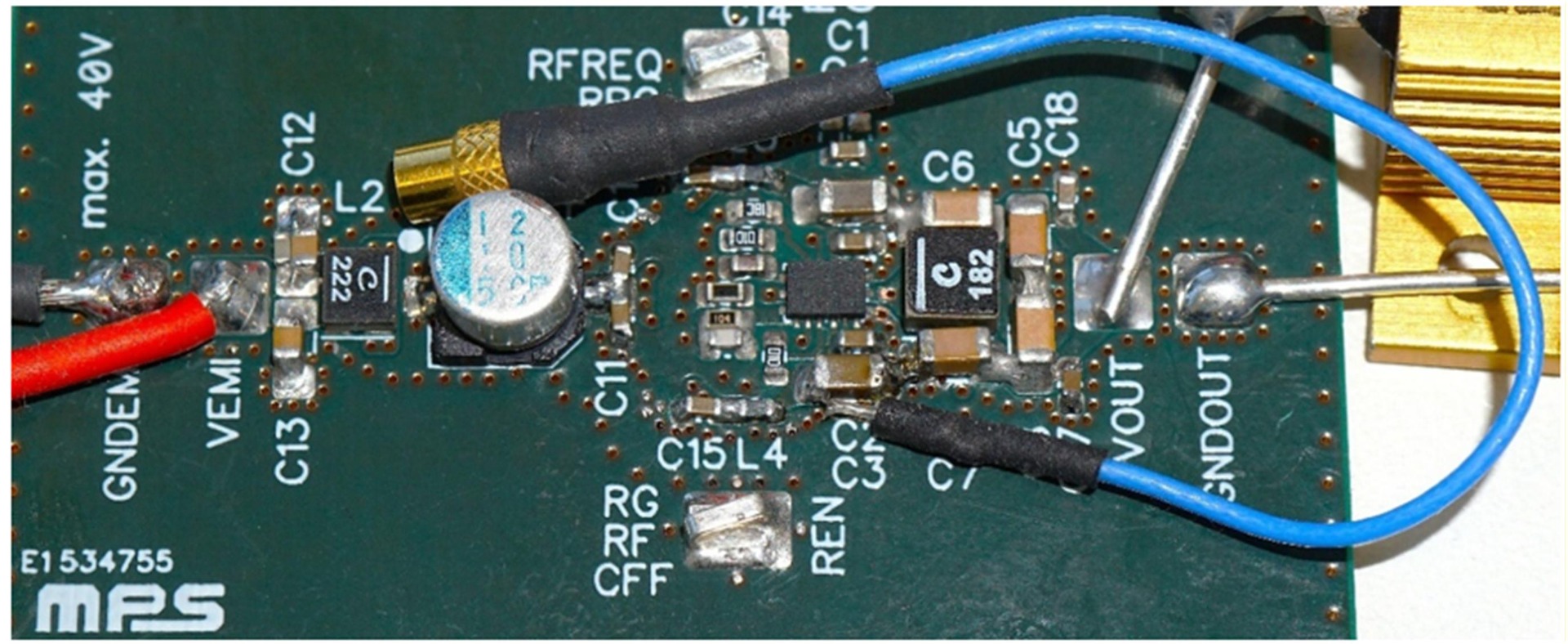
Figure 2: MPQ4324-AEC1 PCB with a Power Rail Probe Connector on a Hot-Loop MLCC





Component Placement of the Switching Inductor, Hot Loops, and Ferrite Bead
Figure 3 shows the placement of the switching inductor (L1), the four hot loops (C1, C2, C3, and C4), and the low-pass ferrite beads (L3 and L4) with the low-pass multi-layer ceramic capacitors (C15 and C16). This symmetrical placement makes it easier to pass stringent automotive EMC specifications such as CISPR 25 Class 5. The four hot loops have a high di/dt, and the parasitic inductance in these hot loops must be kept as low as possible to minimize the ringing amplitude (see Figure 4, Figure 5, and Figure 6).
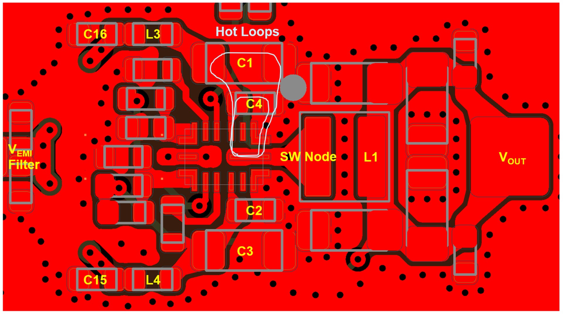
Figure 3: Component Placement for the SW Node and Hot Loops
Table 1 shows the component selection for the SW node and the hot loop in a 2.2MHz switching frequency (fSW) design.
Table 1: Component Selection for 2.2MHz fSW Design
| Reference Designator | Value | Recommendation |
|---|---|---|
| L1 | 1.8µH, RDC = 12.6mΩ, IRMS = 7.2A, 4mmx4mmx2.5mm |
|
| C2, C4, C15, C16 | 100nF, 50V, 0402 |
|
| C1, C3 | 4.7µF, 50V, 1206 | Place C1 and C3 close to C2 and C4. Maximize the capacitances for the selected SMT package size. |
| L3, L4 | 0402, 0.5 x IOUT | Select a ferrite bead with the highest impedance at the measured ringing frequency in Figure 5. |
Measurement on the Switching Inductor (L1)
Figure 4 shows the SW node measured with a 10:1 passive probe, with a 1GHz bandwidth on the probe tip. The switch-node voltage on the SW pin has rising and falling times of about 1ns. With these rising and falling times, the MPQ4324-AEC1 can achieve an efficiency up to 97%.
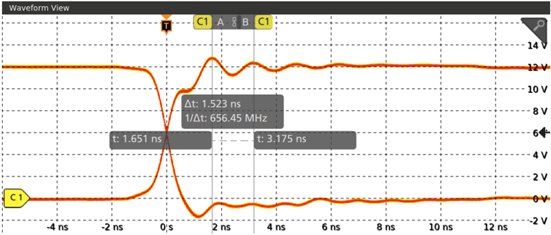
Figure 4: MPQ4324-AEC1 SW Node Measured with a 10:1 Passive Probe
The 656MHz ringing frequency results from a combination of the parasitic series inductances in the hot loop, the hot-loop MLCCs, and the MOSFET transistors’ size and package. Typically, step-down converters with higher nominal currents have a lower ringing frequency (and vice versa). In comparison, the MPQ4371-AEC1 family is available in adjustable versions from 6A to 11A of nominal current, with a ringing frequency of about 270MHz. For VEMI filter design, ferrite beads are well-suited for filtering higher frequencies, while power inductors better cover lower frequency ranges.
Measurements on the Hot-Loop Multi-Layer Ceramic Capacitors (MLCCs)
100nF Hot-Loop MLCC (C2)
Figure 5 shows the 656MHz ringing frequency throughout the PCB with a 300mV peak-to-peak amplitude measured on both pins of the 100nF hot-loop multi-layer ceramic capacitor (C2). The layout must be routed to ensure that the ringing frequency cannot be radiated via unshielded PCB antennas, such as traces, vias, polygons, and components. The EMI voltage (VEMI) filter prevents the frequency spectrum of the rectangular SW node waveform and ringing frequency from being radiated into the wiring harness.
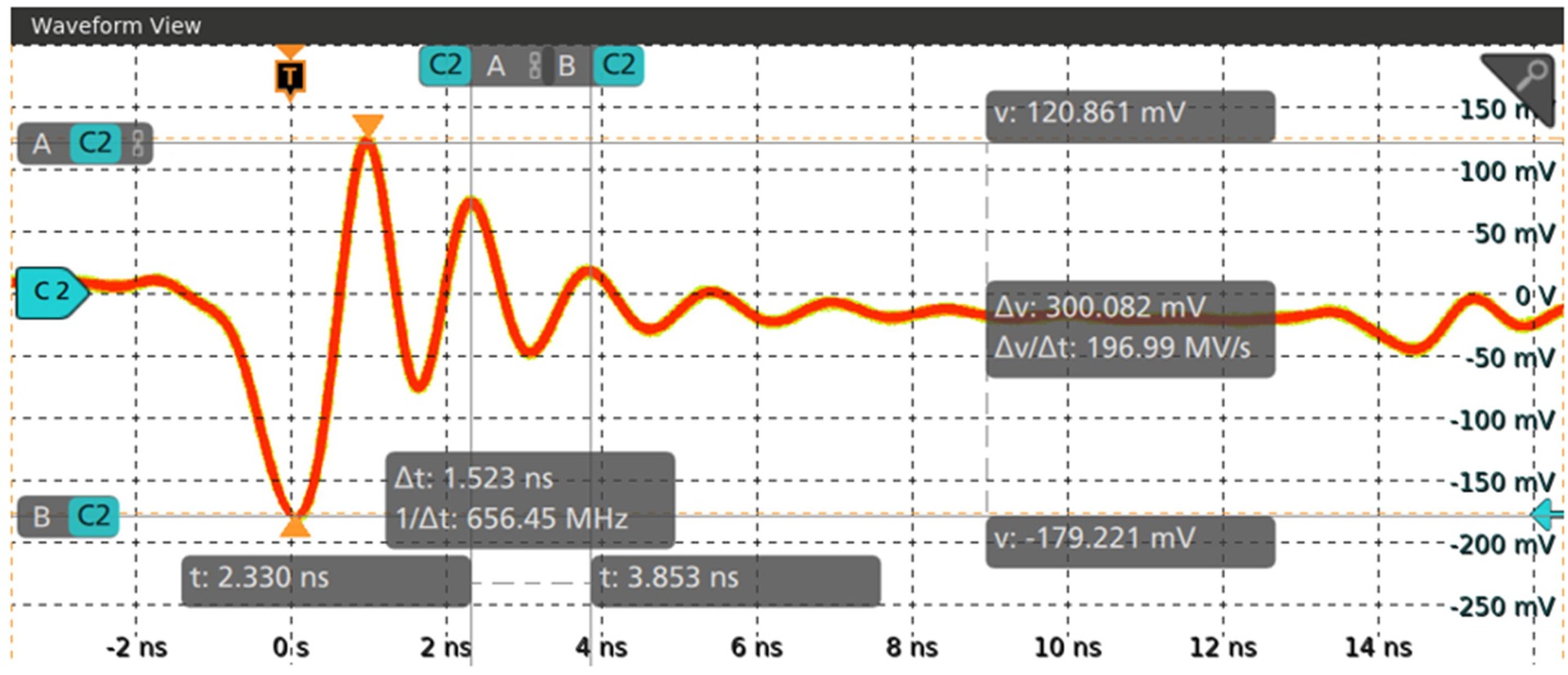
Figure 5: Power Rail Probe of the MPQ4324-AEC1’s 100nF Hot-Loop MLCC (C2)
4.7µF Hot-Loop MLCC (C3)
Figure 6 shows the 656MHz ringing frequency with a 72mV peak-to-peak amplitude measured on the 4.7µF hot-loop multi-layer ceramic capacitor (C3). Although C2 and C3 are connected on the same VIN net, the amplitude at C3 is significantly lower. At 656MHz, the trace between C2 and C3 functions as an inductive series impedance for the low-pass filter with C3, where there is a voltage drop that reduces the amplitude. This demonstrates how correctly placed traces can effectively work as the desired low-pass filter, and reduces the 300mV peak-to-peak amplitude to 72mV for overall lower radiated emissions.
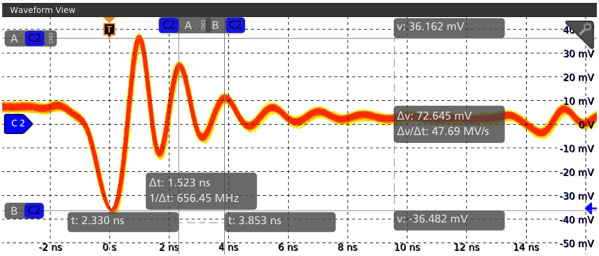
Figure 6: Power Rail Probe of the MPQ4324-AEC1’s 4.7µF Hot-Loop MLCC (C3)
100nF Hot-Loop MLCC (C15)
Figure 7 shows the low-pass filter output of a ferrite bead (L4) measured at the 100nF hot-loop multi-layer ceramic capacitor (C15). The filter attenuates the 656MHz ringing amplitude to a negligible level for EMC, and removes the high frequency in C15. Radiated emissions at 656MHz and comparable frequencies no longer exist in the VEMI filter on traces, vias, components, and in the wiring harness.
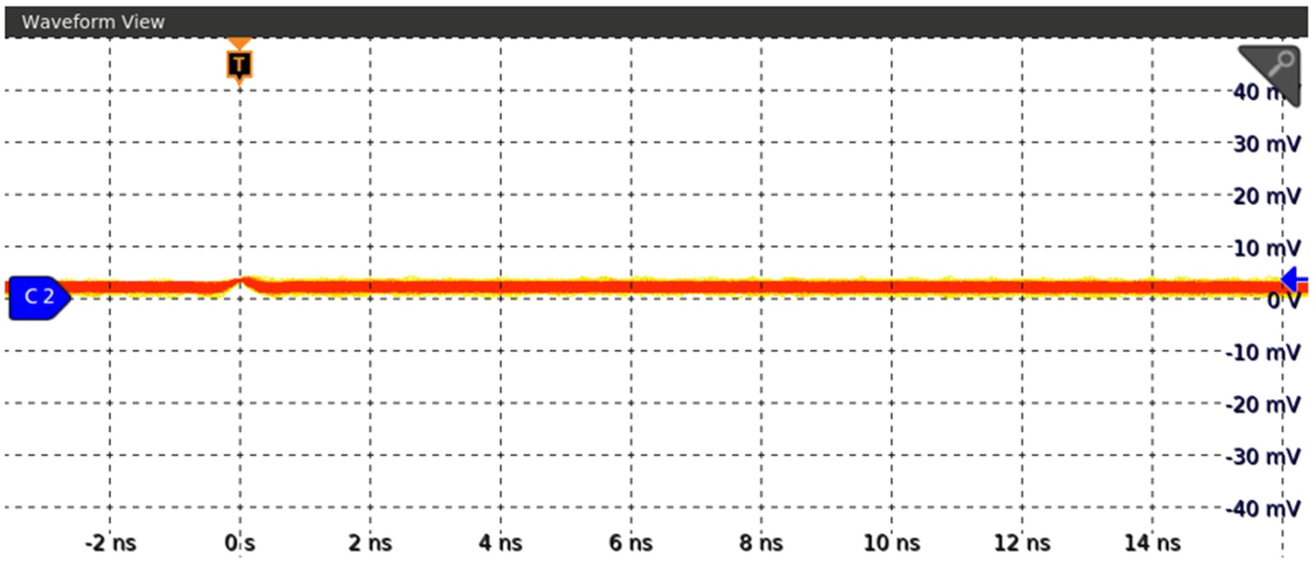
Figure 7: Power Rail Probe of the MPQ4324-AEC1’s 100nF Hot-Loop MLCC (C15)
Significance of the EMI Voltage Filter
The VEMI filter is a two-stage low-pass filter, where MLCCs with ferrite beads attenuate the higher frequencies in the range of several hundred MHz. The power inductor (L2) (see Figure 2) with the MLCCs attenuates the lower frequency ranges. For step-down converters, the filter with the power inductance is more important since CISPR 25 Class 5 requirements cannot be met without the power inductance.
In certain applications, especially at low ringing frequencies (about <300MHz), the ferrite bead can be omitted. A VEMI filter without series impedance (for example, a power inductor and/or ferrite bead) is not able to sufficiently meet CISPR 25 Class 5. The VEMI filter recommendation can usually be found in most datasheets, depending on the application specifications.
Ferrite Bead Placement
There are three possible ferrite bead placements on the PCB, described below:
Two ferrite beads (for example, L3 and L4 in Figure 3) are placed directly next to the hot loops, splitting the VIN current. This decreases the current by half and allows for a smaller package, which can be more expensive than a single ferrite bead with a larger package. The advantage of this PCB placement is that high frequency is filtered directly at the hot loop, preventing propagation to the PCB.
The single ferrite bead can be placed on the right side of the VEMI filter inductor (see L2 in Figure 2), with the advantage of the ringing frequency not reaching the inductor. This prevents the VEMI filter inductor from becoming a radiator or an oscillator stimulated at the ringing frequency. The parasitic inductance and capacitance of the traces and components can form an LC oscillator, which is stimulated by the ringing frequency and the fSW harmonics. The resulting oscillation can increase amplitude and become relevant for EMC through radiation on the VEMI filter’s natural resonant frequency, especially with unshielded traces acting as antenna. A ferrite bead between the IC’s VIN pins and VEMI filter can dampen this effect.
The single ferrite bead filter can be placed on the left side of the power inductor for the advantage of lower VIN inrush currents. For more details, refer to the typical application circuits with the VEMI filter in the MPQ4324-AEC1 datasheet. The VEMI filter inductance is terminated with two 2.2µF MLCCs, which can lead to high inrush currents in the MLCCs. If the ferrite bead filter is placed on the power supply side, then only smaller MLCCs (e.g. 1nF to 10nF) are typically required to be transiently charged, and the ferrite bead can reduce transients in the large 2.2µF x2 MLCCs. These MLCCs combined with the VEMI filter inductor form the low-pass filter. This PCB placement also ensures final filtering against high-frequency leakage into the wiring harness, and is the most commonly used method.
Conclusion
This article explored optimizing EMC filter design and PCB layout using high-frequency ferrite beads to filter out most of the high-frequency interference. For hot loop design, it is recommended to place the multi-layer ceramic capacitors, traces, and vias symmetrically. Additional design recommendations include selecting the ferrite bead with the highest impedance at the ringing frequency, maximizing the capacitance for the SMT package size, and always using a VEMI filter with series impedance. Product datasheets usually include typical application circuits and EMC-tested layouts. It is generally recommended to start EMC testing early in a project to minimize costs for design changes.
To learn more, explore MPS’s robust portfolio of AEC-Q100 qualified switching converters and controllers. MPS also offers support for layout, circuit design, and component selection review, as well as modern EMC laboratories worldwide to support application needs.
_______________________
Did you find this interesting? Get valuable resources straight to your inbox - sent out once per month!
Technical Forum
 Latest activity 3 months ago
 4 Comments
Latest activity 3 months ago
1 Comment
Latest activity 3 months ago
3 Comments
4 Comments
Latest activity 3 months ago
1 Comment
Latest activity 3 months ago
3 Comments
Log in to your account
Create New Account