Comparing the Thermal Behavior of 6A Devices on a Two-Layer Automotive PCB Design

Get valuable resources straight to your inbox - sent out once per month
We value your privacy
Introduction
The rated current is a typical parameter for DC/DC converters, and the maximum possible ambient temperature (TA) depends on the PCB size and the IC’s thermal resistance. In this article, an automotive expert will examine the thermal behavior of MPS’s MPQ4326-AEC1 compared to a traditional 6A device on a small, 2-layer PCB (60mmx40mm).
Using a 2-Layer Layout
The planned production costs and the PCB size determine the required number of layers, typically two layers. In a 2-layer automotive PCB design, the component placement in DC switching power supplies requires careful consideration to meet EMC and thermal specifications.
The Method
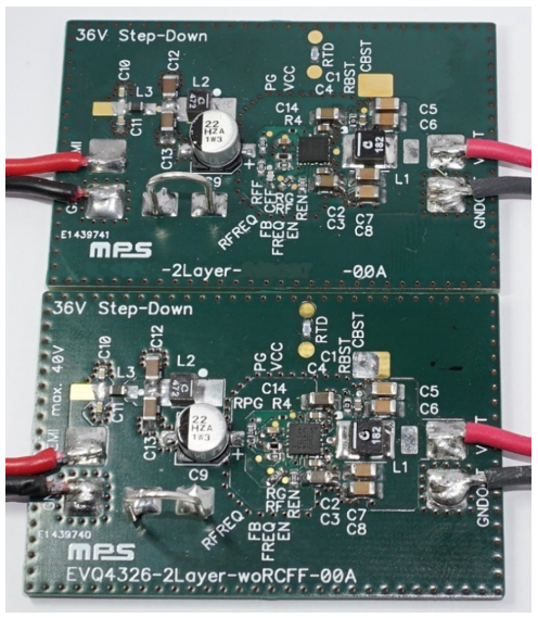
This article tests the closely matching 2-layer layouts of the MPQ4326-AEC1 and a traditional device rated for 6A (see Figure 1). While each layout has unique component positions, the matching placements for the polygons and vias enable a comparison of the differences between the thermal and efficiency performances of these layouts (see Figure 2 and Figure 3).
Figure 1 shows the typical application schematic for the MPQ4326-AEC1, which closely matches a traditional 6A device.

Figure 1: MPQ4326-AEC1 Typical Application Schematic
Both ICs use the same external component package sizes and layout, enabling a true 1:1 comparison for efficiency and thermal performances. Some differing IC-specific values include feedback, the switching frequency resistor, and pinout details.
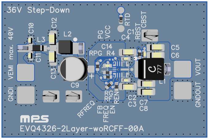
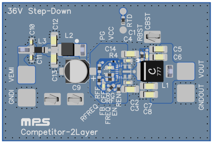
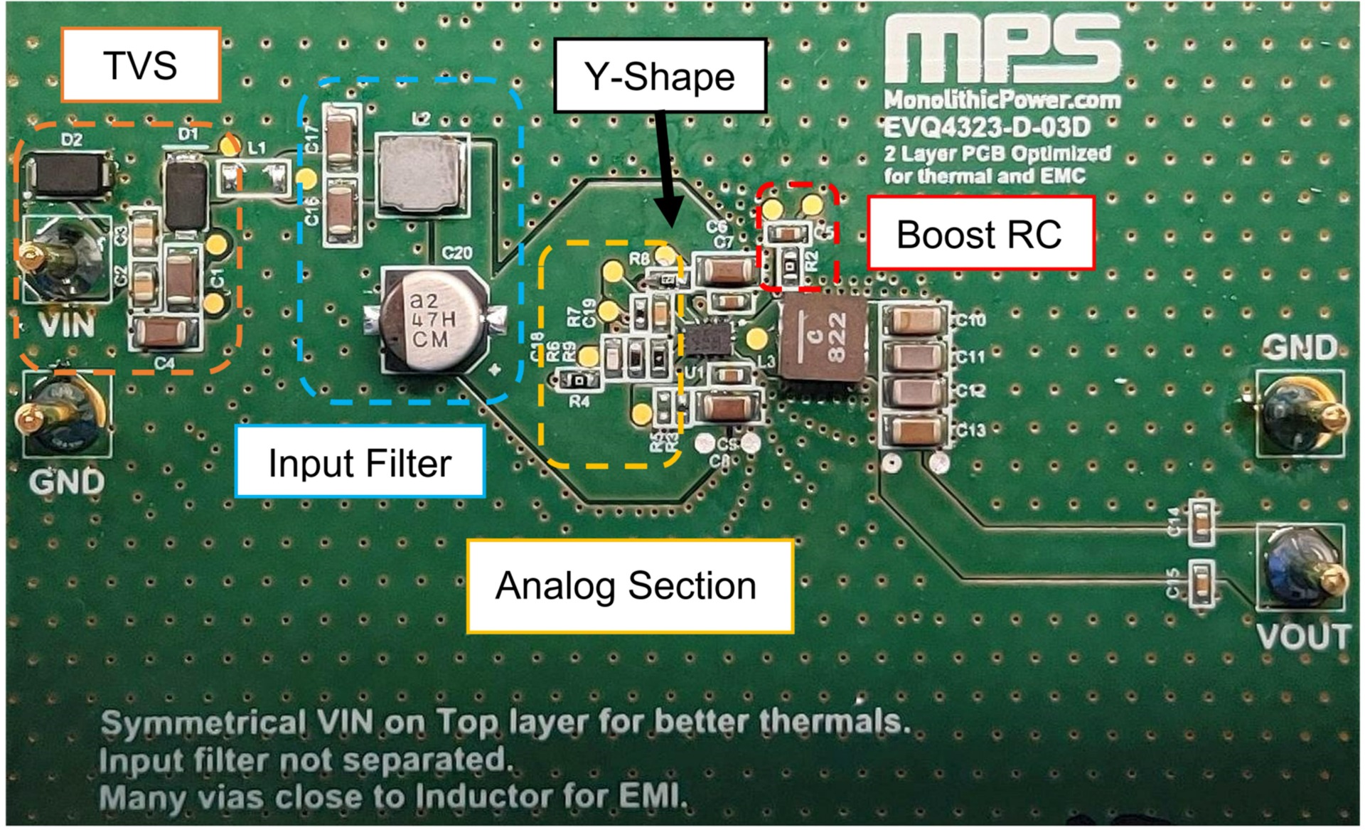
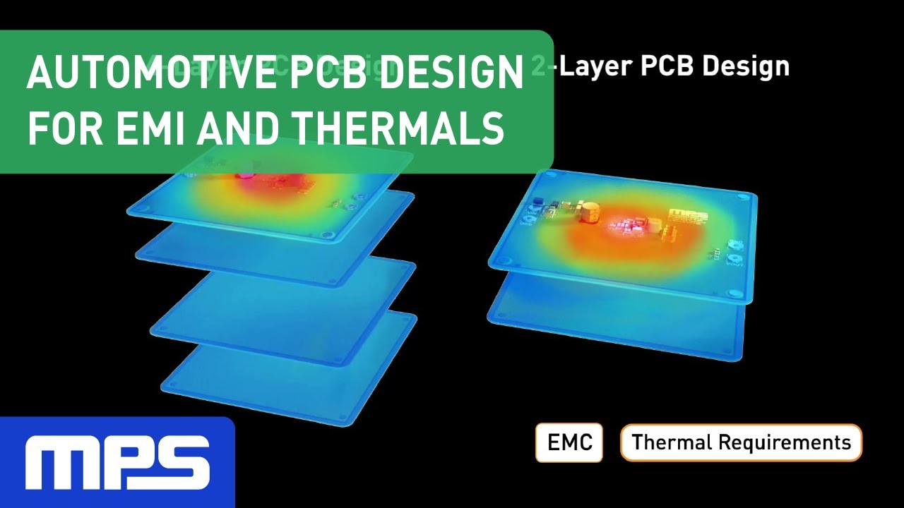
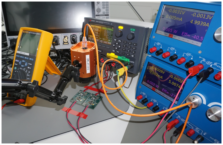
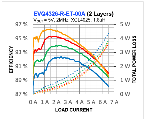
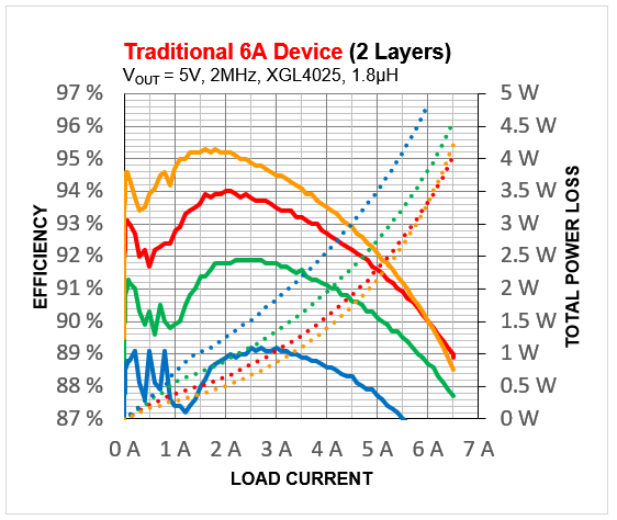
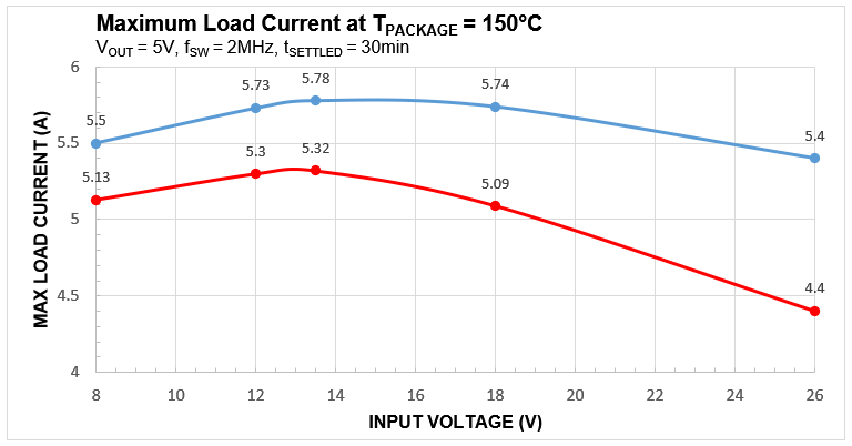
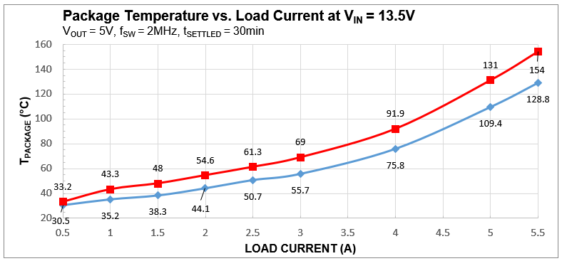
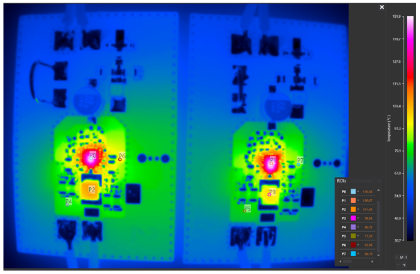
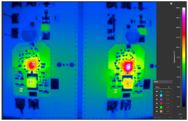
Figure 2 shows the PCB component placement for the MPQ4326-AEC1. Figure 2: MPQ4326-AEC1 2-Layer PCB (60mmx40mm) Component Placement Figure 3 shows the PCB component placement for a traditional 6A device. Figure 3: Traditional 6A Device 2-Layer PCB (60mmx40mm) Component Placement The layout on both PCBs has a common GND plane for the bottom layer as well as a 35µm copper thickness with 1.55mm between the layers on standard FR-4 epoxy. The optional platinum resistance temperature detector (RTD) can measure the PCB temperature. An automotive expert uses MPS’s MPQ4323-AEC1 to provide practical advice on how the schematic and layout designs for 2-layer PCBs can be fine-tuned to achieve the best possible thermal characteristics, and stay well within the standards for CISPR25 Class 5. Learn more about automotive PCB design with our latest video, where we unveil how a cost-effective 2-layer PCB design can meet the rigorous thermal and EMC requirements of modern automotive applications This use case examines the application of the MPQ4323-AEC1 synchronous buck converter in infotainment systems. Learn how to design a 2-layer PCB that will pass automotive EMC and can effectively dissipate heat. Efficiency is defined as a quotient of the electrical power from the output power (POUT) to input power (PIN) of a DC/DC converter. Efficiency is determined by device-specific parameters, application-specific parameters, and PCB-specific parameters, which are described in more detail below: For a proper 1:1 efficiency comparison of the two DC/DC converters, the application and PCB parameters must be the same. Figure 4 shows a comparison of the two PCBs. Figure 4: Comparison of 2-Layer PCBs for the MPQ4326-AEC1 and a Traditional 6A Device Figure 5 shows the set-up to measure the efficiency and the thermal images, where the same power supply drives both PCBs with the same length of power and load cables. Efficiency is measured using four-wire technology for current and voltage. The measuring points are on the electrolytic capacitor for VIN and on the output MLCCs for VOUT. Figure 5: Test Set-Up for Efficiency and Infrared Thermal Images Each PCB can be loaded separately with an adjustable constant current. The IR thermal camera records the temperature profile of both PCBs simultaneously. The PCBs operate at the same conditions with matching surfaces, cables, and air convection, resulting in equal heat dissipation to the ambient temperature. The MPQ4326-AEC1 comes in a QFN-14 (4mmx4mm) package that is rated for ILOAD = 6A and a junction-to-ambient thermal resistance, θJA = 46.7°C/W on a JESD51-7 thermal test PCB. The traditional 6A device comes in a QFN-14 (3.5mmx4mm) package that is rated for ILOAD = 6A and θJA > 46.7°C/W on a JESD51-7 thermal test PCB. θJA allows for a 1:1 heat flow comparison from the die temperature to the ambient temperature when soldered on a JEDEC JESD51-7 test PCB. A smaller θJA enables improved heat flow from the IC package on the PCB to the ambient air temperature. Figure 6 shows the efficiency and total power loss curves for the MPQ4326-AEC1. VIN is 8V for the orange line, 12V for the red line, 18V for the green line, and 26V for the blue line. Figure 6: MPQ4326-AEC1 Efficiency and Total Power Loss on a 2-Layer PCB Figure 7 shows the efficiency and total power loss curves for the traditional 6A device. Similar to Figure 6, VIN is 8V for the orange line, 12V for the red line, 18V for the green line, and 26V for the blue line. Figure 7: Traditional 6A Device Efficiency and Total Power Loss on a 2-Layer PCB Under the same applications and PCB conditions, the MPQ4326-AEC1 achieves higher efficiency and lower total power loss. Thus, the advantage of the MPQ4326-AEC1 at high load currents is clear. Figure 8 shows the maximum achievable ILOAD (ILOAD_MAX) when the package temperature at the top of the IC (TPACKAGE) remains constant at 150°C while sweeping VIN. The blue line represents the MPQ4326-AEC1, and the red line represents the traditional 6A device. Figure 8: Maximum Load Current at TPACKAGE = 150°C Compared to the traditional 6A device, the MPQ4326-AEC1 supports up to 1A of additional ILOAD under the same conditions and TPACKAGE. Figure 9 shows TPACKAGE when sweeping ILOAD, where the blue line represents the MPQ4326-AEC1, and the red line represents the traditional 6A device. Figure 9: Package Temperature vs. Load Current at VIN = 13.5V At ILOAD = 5.5A, the MPQ4326-AEC1’s TJ is below the traditional 6A device’s TJ by 25°C. The advantages of the MPQ4326-AEC1 are significant. Each measurement point is settled for 30 minutes to ensure steady conditions. Figure 10 shows the infrared images of the two PCBs, which each have a different ILOAD_MAX when TPACKAGE reaches 150°C. The thermal images are tested at VIN = 26V, VOUT = 5V, TAIR = 23°C, fSW = 2MHz, and tSETTLED = 30min. ILOAD of each PCB is adjusted to its maximum value until TPACKAGE of both PCBs reaches 150°C. The MPQ4326-AEC1 is shown on the left at ILOAD_MAX = 5.4A and POUT = 27W. The traditional 6A device is shown on the right at ILOAD_MAX = 4.4A and POUT = 22W. Figure 10: MPQ4326-AEC1 vs. Traditional 6A Device at TPACKAGE = 150°C and Different ILOAD_MAX Values Under the same conditions, the MPQ4326-AEC1 can achieve up to 1A of additional output current. The MPQ4326-AEC1’s PCB (left) has a slightly higher temperature caused by the higher POUT and higher input currents. TPACKAGE is the same for both PCBs, indicating the MPQ4326-AEC1 package’s improved efficiency and lower θJA from the silicon to the ambient temperature, mainly in the solder pads. Figure 11 shows the infrared images for TPACKAGE when sweeping ILOAD. The thermal images are tested at ILOAD = 5.5A, POUT = 27.5W, VIN = 13.5V, VOUT = 5V, TAIR = 23°C, fSW = 2MHz, and tSETTLED = 30min. ILOAD increases to its maximum value until TPACKAGE of one of the PCBs reaches 150°C. The MPQ4326-AEC1 is shown on the left at TPACKAGE = 129°C. The traditional 6A device is shown on the right at TPACKAGE = 154°C. Figure 11: TPACKAGE vs. ILOAD of MPQ4326-AEC1 and Traditional 6A Device Under the same conditions, the MPQ4326-AEC1’s TPACKAGE remains 25°C below the traditional 6A device. Measurement stops at ILOAD = 5.5A as the traditional 6A device’s TPACKAGE reaches 154°C. This prevents TPACKAGE from further increasing and causing thermal shutdown. In this article, we made comparative measurements using the MPQ4326-AEC1 and a traditional 6A device, nominally specified for ILOAD = 6A. The specified rated current can be achieved on a small, low-cost PCB with differences in TPACKAGE and ILOAD_MAX. Across the efficiency, maximum load current, package temperature, and thermal measurements, the MPQ4326-AEC1 demonstrates key advantages in efficiency and lower total power loss. The PCB’s size and technology must be adjusted when operating at higher TA values, as the heat flow of the 2-layer (60mmx40mm) PCB is insufficient. Furthermore, the 1:1 comparative test proves that a 6A DC/DC converter cannot consistently deliver a 6A ILOAD, depending on the PCB’s heat flow capability, thermal resistance of the package, and efficiency. MPS products provide specifications for the nominal current. Contact an MPS FAE for more details on optimizing PCBs for application specifications, and explore MPS’s wide selection of switching converters and controllers.
Related Content
A Thermally Optimized, Two-Layer Automotive PCB Design to Meet CISPR25 Class 5
How to Design an Automotive PCB Layout for EMI and Thermals

Step-Down Converter Use Case: Infotainment Systems

Make a Great Automotive PCB for EMC & Thermal
Efficiency Measurement
Device-Specific Parameters
Application-Specific Parameters
PCB-Specific Parameters
Test Set-Up
Comparison of Efficiency Curves
Maximum Load Current vs. Input Voltage at TPACKAGE = 150°C
Package Temperature vs. Load Current at VIN = 13.5V
Thermal Image of Maximum Load Current vs. Input Voltage at TPACKAGE = 150°C
Thermal Image of Package Temperature vs. Load Current at VIN = 13.5V
Conclusion
_______________________
Did you find this interesting? Get valuable resources straight to your inbox - sent out once per month!
Technical Forum
 Latest activity 14 hours ago
 2 Comments
Latest activity 2 weeks ago
3 Comments
Latest activity 3 weeks ago
2 Comments
2 Comments
Latest activity 2 weeks ago
3 Comments
Latest activity 3 weeks ago
2 Comments
Log in to your account
Create New Account