


An Equation-Driven Guide to Designing a CrM/DCM Boost PFC
DOWNLOAD PDF


Get valuable resources straight to your inbox - sent out once per month
We value your privacy
Introduction
Designing compact and efficient power factor correction (PFC) stages for low-power to mid-power applications often requires operating in critical conduction mode (CrM) or discontinuous conduction mode (DCM). These modes offer improved efficiency and simplified control at light loads, but require careful design to ensure correct valley detection and mode transitions across the entire input range and load range.
CrM/DCM boost PFC topology is a highly recommended solution for applications up to 200W. This topology remains a compelling choice for the 200W to 400W range, particularly when cost-effectiveness and light-load performance are primary design constraints. However, it is important to select the most suitable mode depending on the power level and system constraints.
This article presents a step-by-step methodology for designing a boost PFC stage that operates in CrM under worst-case conditions and falls back to discontinuous conduction mode at lighter loads (see Figure 1).
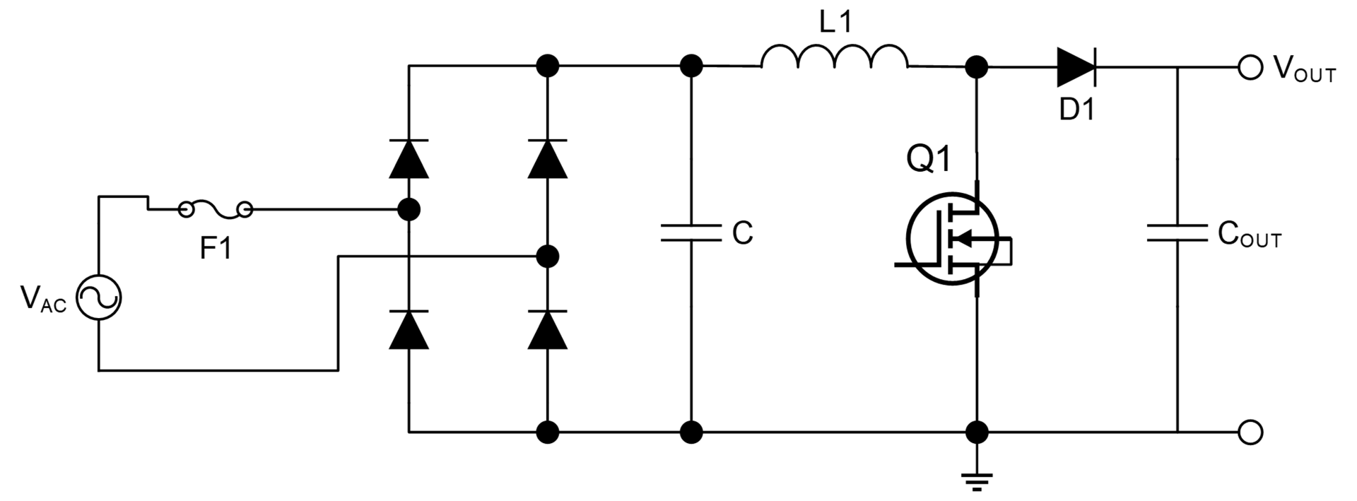
Figure 1: Boost Power Factor Correction Stage
The inductor is selected to achieve critical conduction at the minimum input voltage (VIN) and a full load, ensuring proper zero-current switching. Key aspects such as variable frequency behavior, inductance, and peak current calculation are addressed in this article through a formula-driven approach.
Step 1: Define the Operating Parameters
An effective power design should include a clear set of specifications and consider the worst-case scenario. The operating parameters for a universal input PFC converter are the minimum AC RMS input voltage and maximum output power (POUT_MAX).
Table 1 shows the power converter specifications for a practical example, which will be applied to the following calculations in this article.
Table 1: Power Converter Specifications
| Parameters | Value | Units |
|---|---|---|
| Input voltage (VIN) range | 85 to 265 | VAC |
| Output voltage (VOUT) | 395 | VDC |
| Output power (POUT) | 150 | W |
| Target efficiency | 94 | % |
| Minimum switching frequency (fSW) | 70 | kHz |
Based on Table 1, the minimum switching frequency (fSW) is at the peak of the low AC line and at POUT_MAX. Figure 2 shows that the inductor current dependent on time (iL (t)) follows the AC input voltage and its average value (IL_AVG) in CrM.
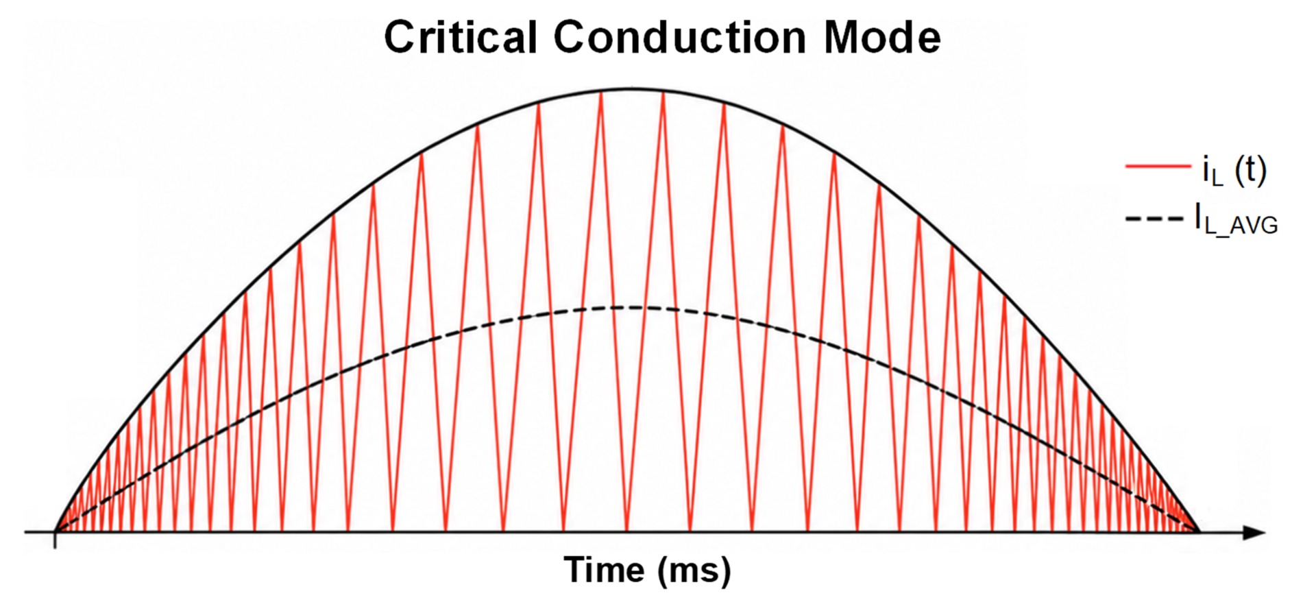
Figure 2: Inductor Current in CrM
The worst-case conditions can be determined using the power converter specifications from Table 1.
The maximum input power (PIN_MAX) can be calculated with Equation (1):
PIN_MAX = POUT_MAXη (1)
If POUT_MAX is 150W and η is 0.94 under the worst-case conditions, then PIN_MAX is 159.57W.
The minimum peak AC voltage (VIN_PK_MIN) can be calculated with Equation (2):
VIN_PK_MIN = VAC_MIN x √2 (2)
If VAC_MIN is 85V, then VIN_PK_MIN is 120.21V.
Step 2: Calculate the Inductance
The single most important component in this design is the boost inductor (L). Figure 3 shows an example of a power inductor for the power factor correction boost stage.
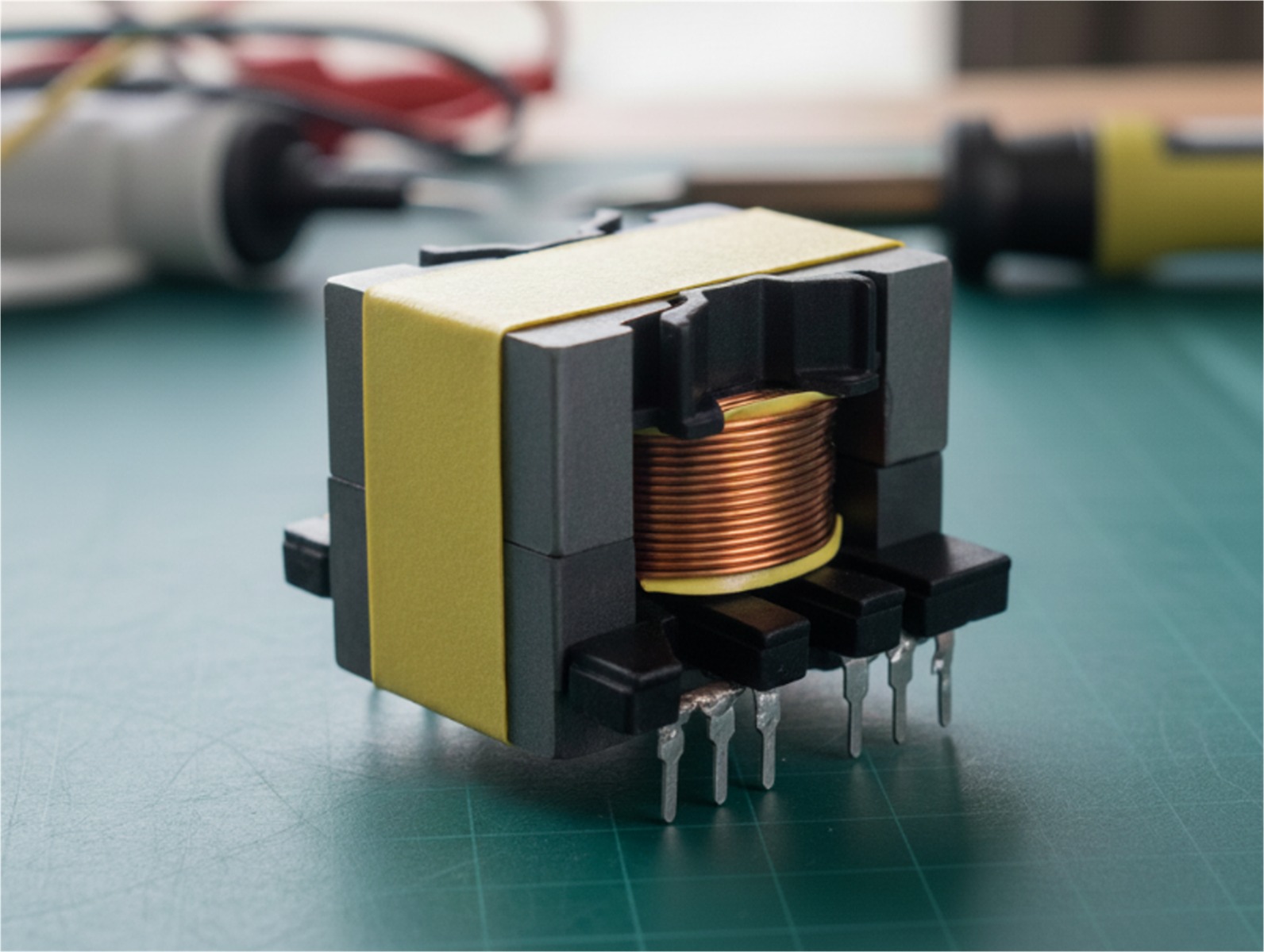
Figure 3: Power Inductor for PFC Boost Stage
The boost inductance determines the energy storage per cycle and mode. The converter must be in CrM at the minimum AC input voltage under full loads. This ensures that the inductor has sufficient energy storage capability for all other operating conditions.
The required inductance (L) for CrM can be calculated with Equation (3):
L = (VIN_PK_MIN)2 x (VOUT - VIN_PK_MIN)2 x PIN_MAX x fSW_MIN x VOUT (3)
Where VIN_PK_MIN is the peak input voltage at the minimum AC input voltage, VOUT is the DC output voltage, PIN_MAX is the input power at full load, and fSW_MIN is the target minimum switching frequency.
The inductance based on Equation (3) and the power converter specifications provided in Table 1 is 450µH, as shown below.
L = (120.21V)2 x (395V - 120.21V)2 x 159.57W x 70000Hz x 395V = 450µH
At the highest current demand (low line peak at full loads), a 450µH inductor ensures that the current returns to 0A by the end of a 70kHz cycle. For any other current demand levels, the cycle completes faster, causing the part to operate in discontinuous conduction mode.
Step 3: Calculate the Maximum Component Stress
With a fixed inductance, the absolute maximum peak current tolerated by the MOSFET and diode at the peak of the low AC line voltage can be calculated. In CrM, the inductor current waveform is a triangle starting from 0A, where the peak current (ISW_PK) is exactly twice the average input current. The average current at the peak of the sinusoid (IIN_PK_AVG) can be calculated with Equation (4):
IIN_PK_AVG = 2 x PIN_MAXVIN_PK_MIN (4)
The absolute peak switch current (ISW_PK_MAX) can be calculated with Equation (5):
ISW_PK_MAX = 2 x IIN_PK_AVG = 4 x PIN_MAXVIN_PK_MIN (5)
The calculation for the practical example is shown below:
ISW_PK_MAX = 4 x 159.57W120.21V ≈ 5.31A
This means that the MOSFET (Q1) and boost diode (D1) must be rated to handle a repetitive peak current of at least 5.31A. The RMS current rating is lower, but this peak value determines the component’s survivability.
Step 4: Analyze Variable Frequency Operation
A defining characteristic of a CrM/DCM PFC is its variable switching frequency (fSW). fSW changes dynamically throughout each half-cycle of the AC line, and is the lowest at the peak of the AC voltage (where the most power is processed) and highest near the zero-crossings.
The instantaneous fsw (t) can be calculated with Equation (6):
fsw (t) = vin (t)2 x (VOUT - vin (t))2 x L x p(t) x VOUT (6)
Where vin (t) is the instantaneous input voltage, and p (t) is the instantaneous input power.
vin (t) can be calculated with Equation (7):
vin (t) = VIN_PK x |sin(ωt)| (7)
p (t) can be calculated with Equation (8):
p (t) = PIN_PK x sin(ωt)2 (8)
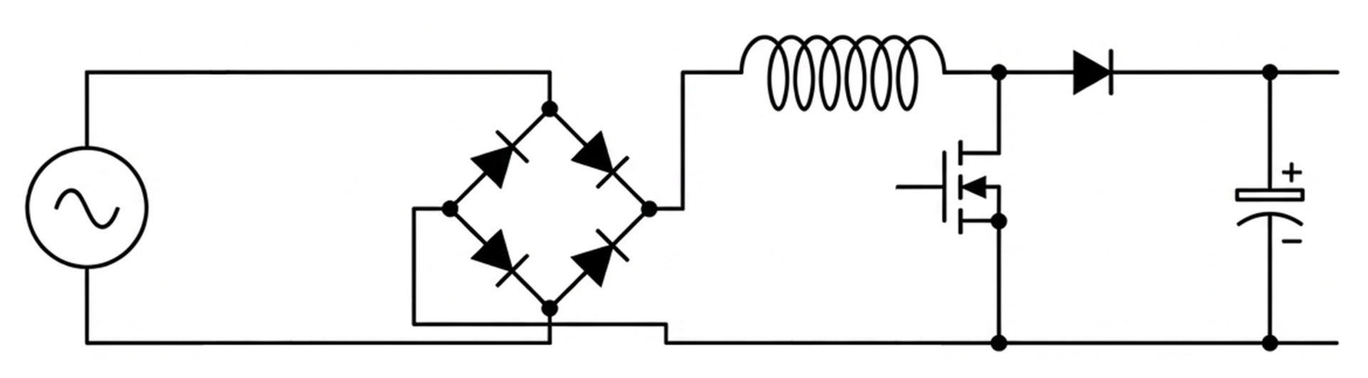

Figure 4 shows fSW across a half-line cycle, which has a characteristic U shape.
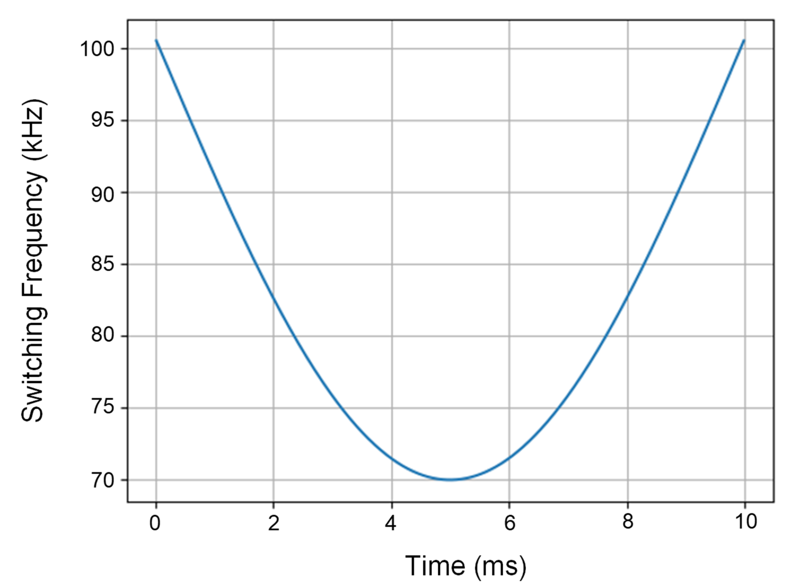
Figure 4: fSW across a Half-Line Cycle
The designed minimum 70kHz switching frequency (fSW_MIN) is lowest at the peak of the sinusoid, while the frequency rises dramatically near the zero-crossing. The controller IC must have a maximum frequency clamp to prevent excessively high-frequency operation, which would lead to high switching losses. A typical clamp is about 250kHz.
Step 5: Understanding the Control Loop and Zero-Current Detection (ZCD)
Compared to a fixed-frequency CCM design, a CrM/DCM PFC uses on-time control and zero-current detection (ZCD). The voltage loop sets the on-time command to regulate the output voltage (VOUT), while the ZCD signal and the controller’s internal timing logic determine when the next switching cycle can begin. As a result, fSW depends on the on time (tON), the inductor demagnetization time, and any additional delay introduced by the controller.
On-Time Control
The main control loop adjusts the MOSFET’s tON. A longer tON results in a higher peak current and more power delivered to the output. The controller's error amplifier (EA) compares VOUT to a reference voltage and sets the required tON to keep VOUT in regulation. The tON behavior across the AC line cycle depends on the control method implemented between constant-on-time (COT) control and variable-on-time (VOT) control.
- Constant-on-time (COT): In this standard approach, the controller maintains a fixed tON throughout a single mains half-cycle. The peak current (IPK) can be calculated with Equation (9):
IPK = vin (t) x tONL (9)
The current naturally follows the sinusoidal shape of VIN, providing inherent power factor correction. The voltage loop updates this constant value slowly across several cycles to regulate the output load.
- Variable-on-time (VOT): To further minimize total harmonic distortion (THD), advanced controllers may modulate tON within the half-cycle. For example, intentionally extending tON near the VIN zero-crossings can compensate for dead zones and crossover distortion, resulting in a purer sinusoidal input current.
Zero-Current Detection (ZCD)
Rather than use a fixed-frequency clock to start a new cycle, the controller waits for a signal from the ZCD circuit indicating that the inductor current (IL) has dropped to 0A. An auxiliary winding is added to the boost inductor. When IL decays and reaches 0A, the voltage on the main winding collapses, inducing a voltage swing in the auxiliary winding. This voltage swing is detected by the ZCD pin on the PFC controller, which immediately initiates the next MOSFET turn-on event.
Final Design
By calculating the required boost inductance and current on the semiconductor devices, a power factor correction boost converter design can be completed using the MP44020, a multi-mode CrM/DCM PFC controller. Table 2 shows the key design results for a 150W application.
Table 2: Design Results for a 150W Application
| Parameters | Value | Units |
|---|---|---|
| Input voltage (VIN) | 85 to 265 | VAC |
| Output voltage (VOUT) | 395 | VDC |
| Output power (POUT) | 150 | W |
| Magnetizing inductance | 450 | µH |
| Maximum peak current | 5.31 | A |
The MP44020 provides simple and high-performance active PFC using minimal external components. To enhance system performance across all load conditions, fSW is reduced at light loads via dead time (DT) extension technology, which improves efficiency and helps achieve very low standby power consumption. The MP44020 also achieves lower THD by implementing VOT control, a significant advantage over conventional COT methods.
Protections include over-voltage protection (OVP), over-current limit (OCL), brown-in (BI) and brown-out (BO), VCC voltage (VCC) under-voltage lockout (UVLO), and over-temperature protection (OTP).
Due to the MP44020’s high integration, the PFC stage requires only a few external components to function effectively. Figure 5 shows the PFC boost converter schematic using the MP44020.
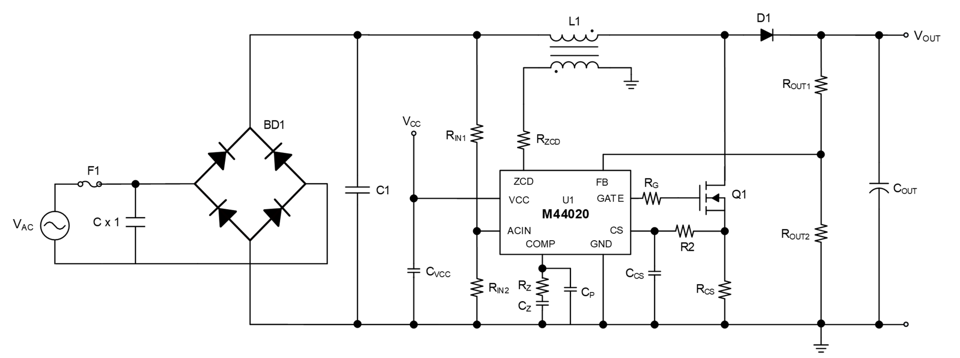
Figure 5: PFC Boost Converter Using the MP44020
Conclusion
Implementing an active power factor correction (PFC) boost converter is a critical first stage for modern AC/DC power supplies. This ensures compliance with harmonic current standards and maximizes power quality. In particular, critical conduction mode (CrM) topology offers a cost-effective solution for applications up to about 400W.
By adhering to the design principles for CrM, such as selecting the appropriate boost inductor and managing the variable fSW, engineers can design efficient and reliable PFC circuits. Moreover, a modern controller like the MP44020 significantly simplifies this task. The MP44020’s variable-on-time (VOT) control scheme ensures low THD in addition to integrated protections and efficiency-boosting features for light-load conditions that achieve a robust and high-performance design.
For more solution options, explore MPS’s selection of integrated, high-performance PFC controllers.
_______________________
Did you find this interesting? Get valuable resources straight to your inbox - sent out once per month!
Technical Forum
 Latest activity 4 months ago
 2 Comments
Latest activity 5 months ago
2 Comments
Latest activity 5 months ago
2 Comments
Log in to your account
Create New Account