MEZS7-PDPowerbank-MP2651 Reference Design
DOWNLOAD THE FULL REFERENCE DESIGN

Get valuable resources straight to your inbox - sent out once per month
We value your privacy
Description
The MEZS7-PDPowerBank-MP2651 is a complete solution module for dual-role ports (DRP) applications, featuring the MP2651 and MPF52002.
The MP2651 is a buck-boost charger IC designed for battery packs with 1 to 4 cells in series, and has a wide 4V to 22V input voltage (VIN) range. In source mode, it can supply a wide 5V to 21V VIN range with the IN pin to comply with USB power delivery (PD) specifications, and has a high-resolution output current limit.
The MPF52002 is a highly integrated USB PD controller for DRP or sink ports, and integrates a 32-bit ARM Cortex-M0 microcontroller (MCU). The controller features automatic DRP toggling for DRP applications, and is compliant with PD3.1 specifications. For source mode, it supports PD3.1, BC1.2, Apple divider mode, Huawei FCP/SCP, and QC2.0/3.0.
The board contains a DRP USB Type-C port, supporting PD3.1 and BC1.2 protocols. When an adapter is inserted, the port acts as a sink port to charge the battery with up to 6A of charge current. When a load is inserted, the port acts as a source port to power the USB VBUS from the battery.
Performance Summary (1)
Specifications are at TA = 25°C, unless otherwise noted.
| Parameters | Conditions | Default Value |
| Sink Mode | ||
| Input voltage (VIN) range | 4V to 22V | |
| Input current(IIN) limit | Up to 5A | |
| Battery charge regulation voltage (VBATT_REG) (2) | 8.4V | |
| Fast charge current (2) | VIN = 9V to 20V | 3A |
| Charge typical efficiency | VIN = 20V, VBATT = 8V, ICC = 3A |
92.2% |
| Source Mode | ||
| Battery voltage range (VBATT) | Up to 18.68V | |
| Output voltage in source mode (VIN_SRC) (3) | 5V to 21V | |
| Default PDO output (2) | 5V/3A, 9V/3A, 15V/1.8A, 20V/1.35A, 5V to 5.9V/3A, 5V to 11V/3A, 5V to 16V/1.8A | |
| Source mode typical efficiency | VBATT = 8V, VIN_SRC = 9V, IIN_SRC = 2.6A | 93.6% |
1) Refer to the MP2651 datasheet for more details.
2) These parameters can be configured by the MPF52002 via the I2C interface.
3) These parameters are configured automatically by the MPF52002, according to protocol.
Evaluation Board
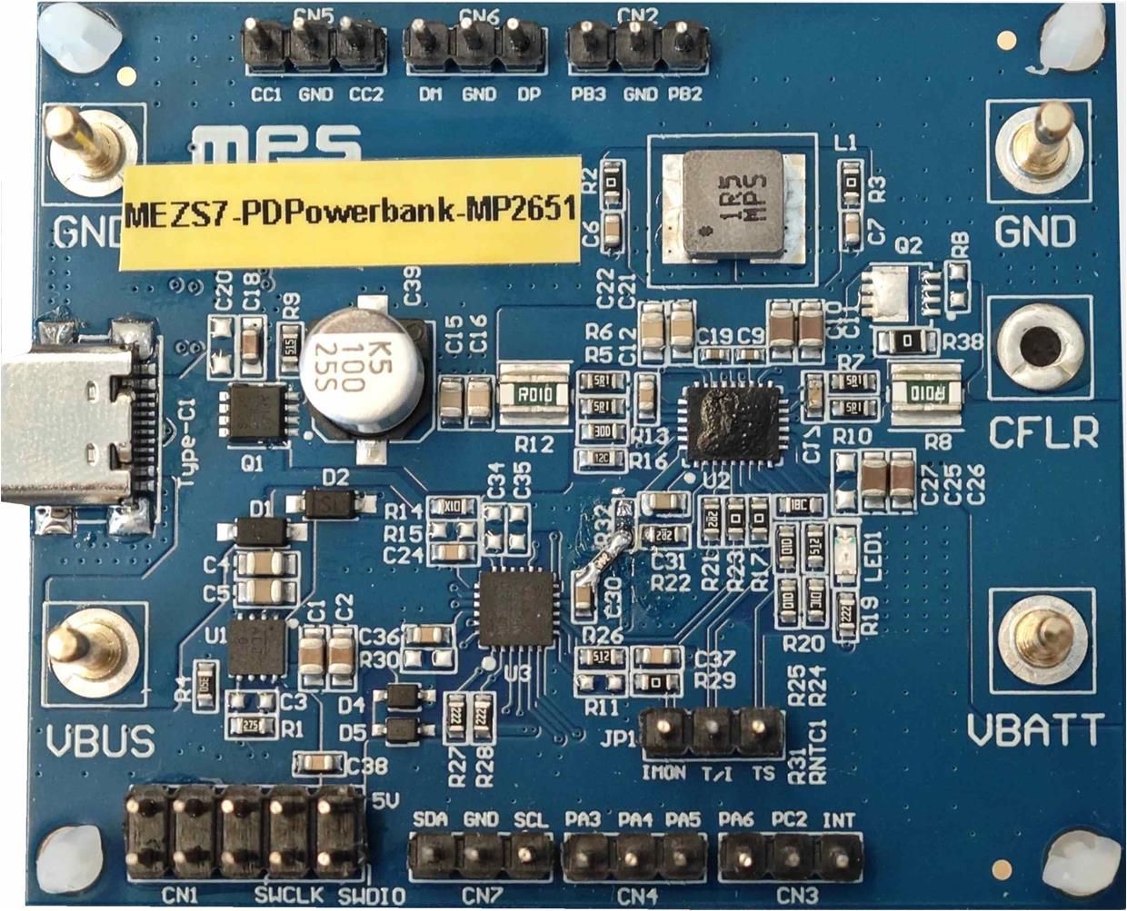
LxWxH (6cmx5cmx2.1cm)
| Board Number | MPS IC Number |
| MEZS7-PDPowerBank-MP2651 | MPF52002GRE-0001 |
| MP2651GVT-000A |
Table 1: Battery Cell Number Setting (4)
| Cell Number | PB2 | PB3 |
| 2-Cell (Default) | 1: Float or high | 1: Float or high |
| 3-Cell | 0: Short to GND | 1: Float or high |
| 4-Cell | 1: Float or high | 0: Short to GND |
4) Set PB2 and PB3 to configure the number of cells before charging a real battery.
Quick Start Guide
The MEZS7-PDPowerBank-MP2651 solution module is a reference design for USB PD applications, and includes a DRP USB Type-C port. The charge current is preset to 3A, and the charge-full voltage is preset to 8.4V for a 2-cell series Li-ion battery. In reverse source mode, the output is preset at 5V/3A or 27W PD.
The user can download their own charge parameter settings to the MPF52002’s volatile memory via the I2C after start-up. Data in the volatile memory resets when the part turns off. The user can also download these parameters to the MPF52002’s non-volatile memory (NVM). Data in the NVM does not reset even when the part turns off.
To prepare the battery connections for testing, follow the steps below:
- Connect the series battery terminals to:
- Positive (+): VBATT
- Negative (-): GND
- If a battery simulator is used:
- Preset the battery voltage, then turn off the simulator.
- Connect the battery simulator output terminals to:
- Positive (+): VBATT
- Negative (-): GND
- Turn the battery simulator on.
- PD3.1 V1.8
- For a non-PD adapter, the bus voltage (VBUS) is 5V. The default input current (IIN) limit is 900mA. If there is a RP on source CC termination, the IIN limit can rise to 1.5A or 3A, according to the RP value.
- PD3.1 V1.8
- DCP
- Apple mode
- Short the INT pin in CN3 (PB1) to GND.
- Connect a USB Type-C device or adapter to the USB Type-C port.
- The initiator SCL clock frequency is 400kHz (fast mode), compliant with the 100kHz to 400kHz clock.
- Read or write 1 byte in every command. The MPF52002 does not support read/write multiple bytes.
- It is recommended to have a 10ms or longer delay between I2C commands.
Before plugging in the adapter, ensure that the settings for PB2 and PB3 are correct (see Figure 1). Otherwise, the system load and battery may be damaged.
Sink Mode
The MPF52002 automatically requests the maximum input power (PIN) according to the adapter’s protocol. Connect the USB Type-C port to an adapter with either a USB Type-C to USB Type-C or a USB Type-A to USB Type-C cable. The MP2651’s input current (IIN) limit and adapter’s output voltage (VOUT) are set according to the protocol. After that, the device will start the charge operation. For 2-cell applications, the default battery full regulation voltage is 8.4V, and the charge current limit is set to 3A.
The default firmware of the MPF52002 on this evaluation board supports the following protocols in sink mode:
The charge current may be limited by the input power (PIN). If the maximum adapter output power is less than the MEZS7-PDPowerbank-MP2651’s output power (POUT), the IIN limit loop adjusts the charge current to avoid overloading the source adapter.
Figure 1 shows the set-up for sink mode.
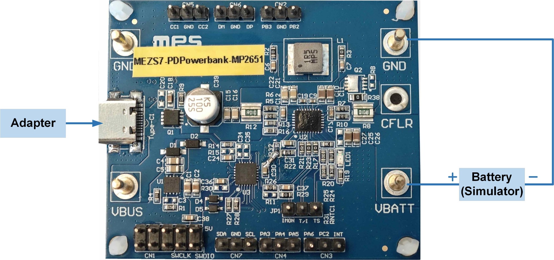
Figure 1: Sink Mode Set-Up
Source Mode
Connect the devices to a USB Type-C port using a USB Type-C to USB Type-C, USB Type-C to micro-B, or USB Type-C to lighting cable. Source mode can start automatically and provide proper voltage to the devices as requested.
The default firmware for the MPF52002 on this evaluation board supports the following protocols in source mode:
VBUS starts up automatically at the voltage set by the PD protocol sniffer or mobile device. The PD protocol sniffer can select different PDO outputs. The default PD output power (POUT) is 27W. The battery discharge current limit is 6.4A.
Figure 2 shows the set-up for source mode.
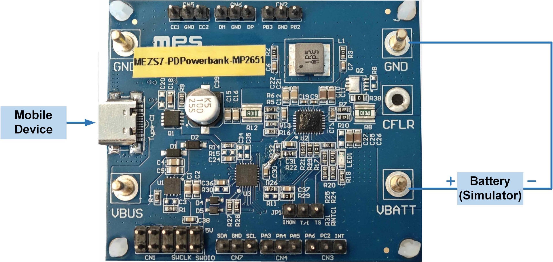
Figure 2: Source Mode Set-Up
I2C Target Function Description
The MP2651 and the MPF52002 can be controlled or monitored via the I2C between the MPF52002 and the I2C initiator. The initiator should connect to the MPF52002 via PB6 and PB7 instead of the MP2651 (see Figure 3). The MPF52002 periodically reads the charge parameters, alerts the status of the MP2651, and updates the information to the I2C target registers. The initiator can also send some I2C commands to the MP2651 through the MPF52002.

Figure 3: MPF52002 I2C Target Diagram Block
I2C Connection Hardware Set-Up
In only battery mode, the MPF52002 can enter deep sleep to save power, and the I2C target registers are disabled. There are two methods to turn the I2C target function back on:
Next, connect the PC and the MEZS7-PDPowerbank-MP2651 with the EVKT-USBI2C-02 communication interface (5) (see Figure 4). The I2C SCL line should be connected via PB6, which has the SWDIO silkscreen print, and the I2C SDA line should be connected on PB7, which has the SWCLK silkscreen print.
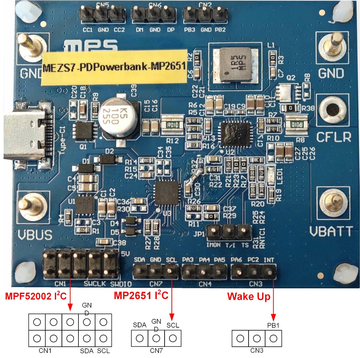
Figure 4: Hardware Connected for the I2C Communication
5) Contact an MPS FAE or request through the MPS website to obtain the EVKT-USBI2C-02 communication interface.
Time Requirements for the I2C Initiator
Evaluation Board Schematic (6) (7)
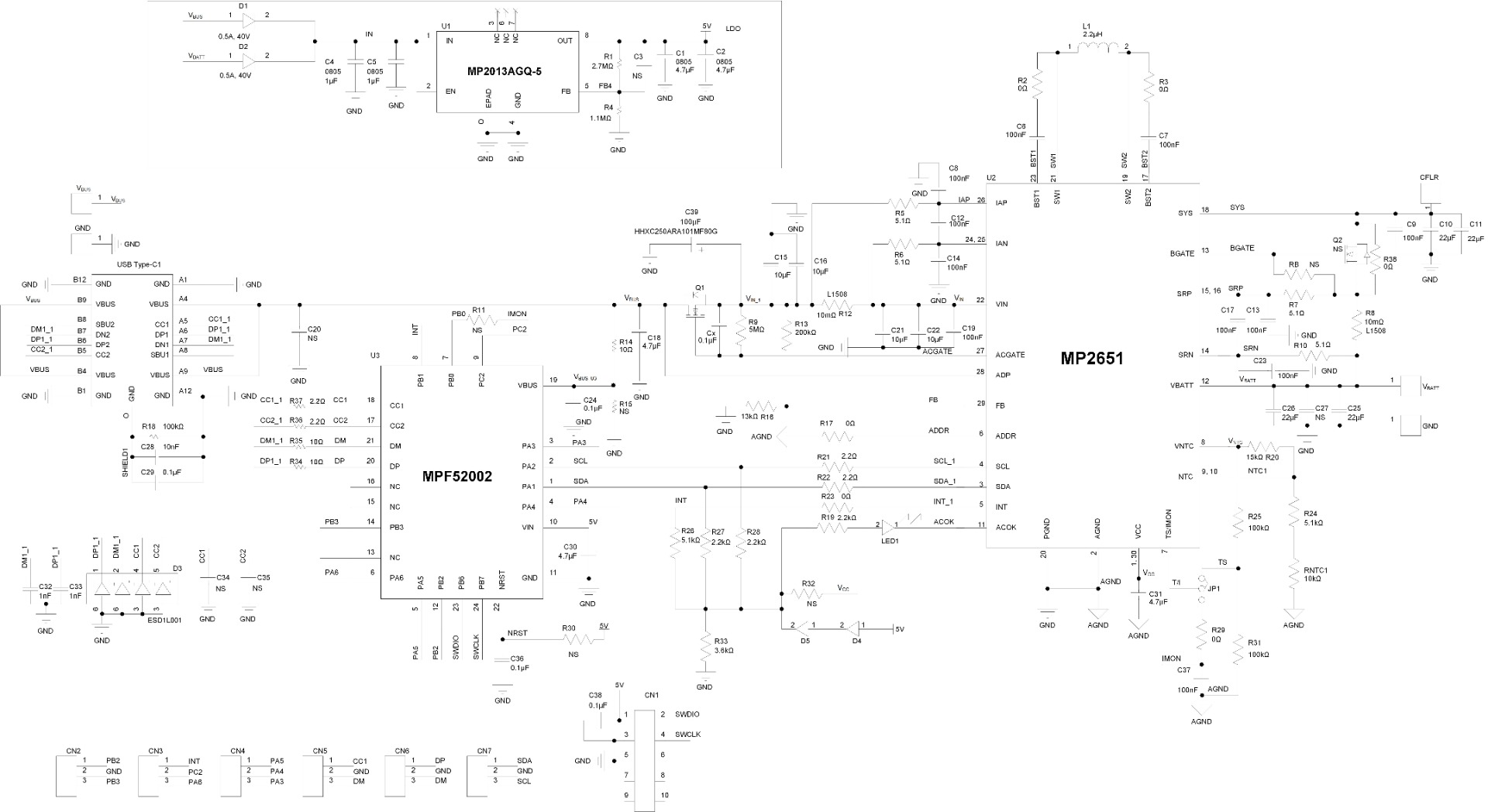
Figure 5: Evaluation Board Schematic
6) A 0.1μF capacitor (Cx) can be paralleled on R9 to avoid inrush current when ACGATE turns on the MOSFET Q1.
7) PB6/7 can be used as the SWD interface. Before downloading any new firmware with the SWD interface, pull PA3 (boot 0) down to restart the MPF52002. When the firmware update is finished, disconnect PB6/7 from the SWD interface and release PA3, then turn the device on to load the new firmware
MEZS7-PDPowerbank-MP2651 Bill Of Materials
| Qty | Ref | Value | Description | Package | Manufacturer | Manufacturer PN |
| 2 | C1, C2 | 4.7μF | Ceramic capacitor, 16V, X7R | 0805 | Murata | GCM21BR71C475KA73L |
| 5 | C3, C20, C27, C34, C35 | NS | ||||
| 2 | C4, C5 | 1μF | Ceramic capacitor, 25V, X7R | 0603 | Wurth | 885012207078 |
| 13 | C6, C7, C8, C12, C13, C14, C17, C23, C24, C29, C36, C37, C38 | 100nF | Ceramic capacitor, 25V, X7R | 0603 | Wurth | 885012206071 |
| 2 | C9, C19 | 100nF | Ceramic capacitor, 25V, X7R | 0402 | Murata | GRM155R71E104KE14D |
| 4 | C10, C11, C25, C26 | 22μF | Ceramic capacitor, 25V, X5R | 0805 | Murata | GRM21BR61E226ME44L |
| 4 | C15, C16, C21, C22 | 10μF | Ceramic capacitor, 25V, X7S | 0805 | Murata | GRM21BC7E106KE11L |
| 1 | C18 | 4.7μF | Ceramic capacitor, 25V, X5R | 0603 | Murata | GRM188R61E475KE11D |
| 1 | C28 | 10nF | Ceramic capacitor, 25V, X7R | 0603 | TDK | C1608X7R1E103K |
| 2 | C30, C31 | 4.7μF | Ceramic capacitor, 16V, X5R | 0603 | Murata | GRM188R61C475KE11D |
| 2 | C32, C33 | 1nF | Ceramic capacitor, 25V, C0G | 0603 | Murata | GRM1885C1E102JA01D |
| 1 | C39 | 100μF | Hybrid, 25V, 20mΩ | SMD | Nippon Chemi-Con | HHXC250ARA101MF80G |
| 1 | R1 | 2.7MΩ | Film resistor, 1% | 0603 | Yageo | RC0603FR-132M7L |
| 5 | R2, R3, R17, R23, R29 | 0Ω | Film resistor, 5% | 0603 | Yageo | RC0603JR-070RL |
| 1 | R4 | 1.1MΩ | Film resistor, 1% | 0603 | Yageo | RC0603FR-071M1L |
| 4 | R5, R6, R7, R10 | 5.1Ω | Film resistor, 1% | 0603 | Yageo | RC0603FR-075R1L |
| 2 | R8, R12 | 10mΩ | Current-sensing resistor, 1%, long side, 1W | L1508 | Film Tech | RL3720WT-R010-F |
| 1 | R9 | 5.1MΩ | Film resistor, 5% | 0603 | Yageo | RC0603FR-075M1L |
| 5 | R11, R15, R30, R32, RB | NS | ||||
| 1 | R13 | 200kΩ | Film resistor, 1% | 0603 | Yageo | RC0603FR-07200KL |
| 3 | R14, R34, R35 | 10Ω | Film resistor, 1% | 0603 | Yageo | RC0603FR-0710RL |
| 1 | R16 | 13kΩ | Film resistor, 1% | 0603 | Yageo | RC0603FR-0713KL |
| 3 | R18, R25, R31 | 100kΩ | Film resistor, 1% | 0603 | Yageo | RC0603FR-07100KL |
| 3 | R19, R27, R28 | 2.2kΩ | Film resistor, 5% | 0603 | Liz | CR0603JA0222G |
| 1 | R20 | 15kΩ | Film resistor, 1% | 0603 | Yageo | RC0603FR-0715KL |
| 4 | R21, R22, R36, R37 | 2.2Ω | Film resistor, 1% | 0603 | Yageo | RC0603FR-072R2L |
| 2 | R24, R26 | 5.1kΩ | Film resistor, 1% | 0603 | Yageo | RC0603FR-075K1L |
| 1 | R33 | 3.6kΩ | Film resistor, 5% | 0603 | Liz | CR0603JA0362G |
| 1 | R38 | 0Ω | Film resistor, 5% | 0805 | Yageo | RC0805FR-070RL |
| 1 | RNTC1 | 10kΩ | Film resistor, 1% | 0603 | Yageo | RC0603FR-0710KL |
| 7 | JP1, CN2, CN3, CN4, CN5, CN6, CN7 | 2.54mm | 3-pin, 1-row | DIP | Wurth | 61300311121 |
| 1 | CN1 | 2.54mm | 5-pin, 2-row | DIP | Wurth | 61301021121 |
| 1 | TYPE_C1 | USB | USB Type-C receptacle, 16-pin | SMD | Yuehu Electronics | PC-071603863-R |
| 4 | VBUS, GND, VBAT | Φ2.0 | Copper pin | DIP | ||
| 1 | CFLR | NS | ||||
| 1 | LED1 | Red | LED | 0805 | Wurth | 150080RS75000 |
| 2 | D1, D2 | IR = 20µA | Schottky diode, 0.5A | SOD123 | AUK | SDB0540 |
| 1 | D3 | 5V | ESD diode | SOT-363 | onsemi | ESD1L001 |
| 2 | D4, D5 | VF = 0.4V when IF = 1mA | 60V, 15mA | SOD-323 | Diodes, Inc. | SD101AWS |
| 1 | Q1 | 8.5mΩ | MOSFET | PowerPAK1212-8 (3.3mmx3.3mm) | Vishay | SISA14DN-T1-GE3 |
| 1 | Q2 | NS | MOSFET | |||
| 1 | L1 | 1.5μH | Inductor, 9.7mΩ, 9A | SMD | MPS | MPL-AL5030-1R5 |
| 1 | U1 | MP2013A | Low-power linear regulator | QFN-8 (3mmx3mm) | MPS | MP2013AGQ-5 |
| 1 | U2 | MP2651 | Buck-boost charger for battery packs with 1 to 4 cells in series | TQFN-30 (4mmx5mm) | MPS | MP2651GVT-000A |
| 1 | U3 | MPF52002 | Highly integrated USB PD controller with a 32-bit ARM Cortex-M0 microcontroller | QFN-24 (4mmx4mm) | MPS | MPF52002-0001 |
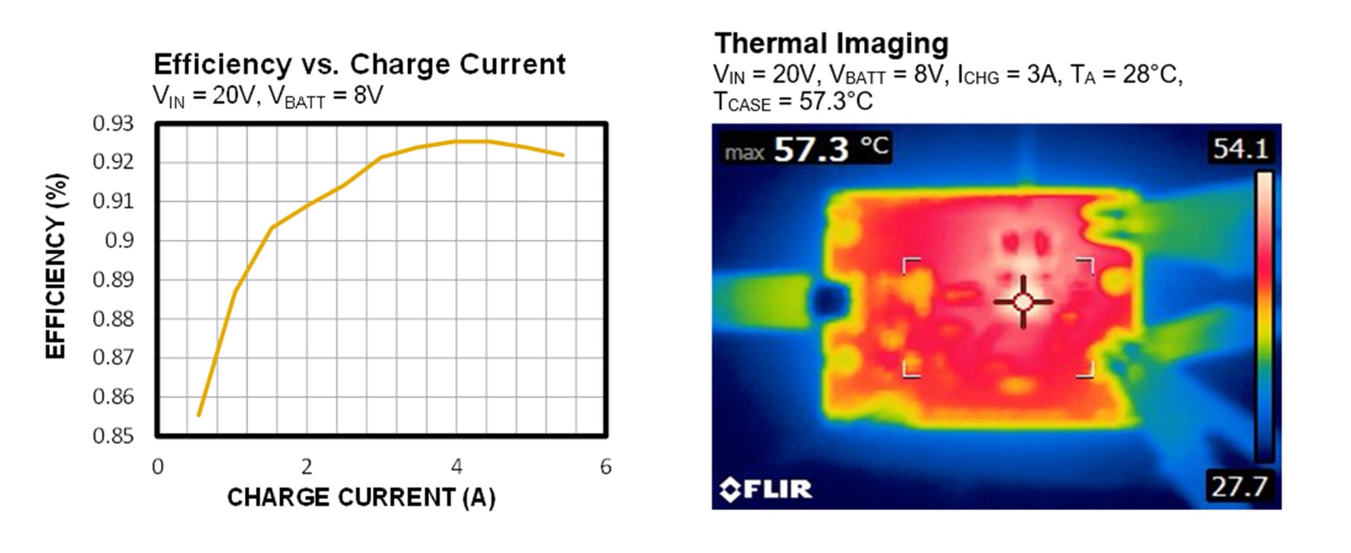
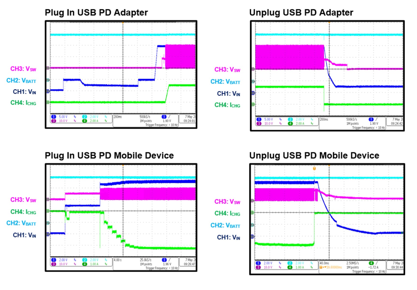
EVB Test Results
Performance curves and waveforms are tested on the evaluation board. The input power source is a USB PD adapter, VIN = 20V, VBATT = 8V, TA = 25°C, default register data, unless otherwise noted.
PCB Layout
Figure 6: Top Layer
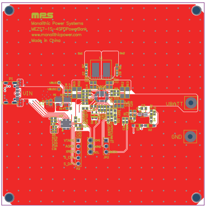
Figure 7: Mid-Layer 1
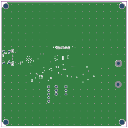
Figure 8: Mid-Layer 2
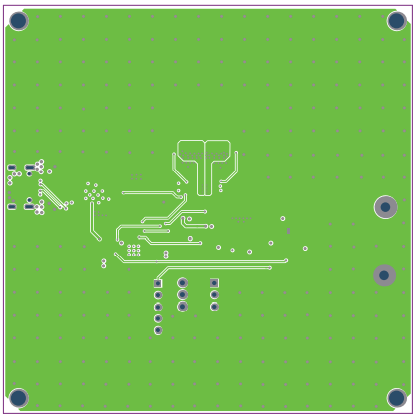
Figure 9: Bottom Layer
Log in to your account
Create New Account