AN043 - Flyback Converter Using Variable Off-Time Controller: HFC0300

Get valuable resources straight to your inbox - sent out once per month
We value your privacy
Abstract
This paper presents design guidelines for flyback converter using variable off-time controller-HFC0300 from MPS as shown in Figure 1. Design of a flyback converter with variable off time (or quasi fixed on time) control is quite simple and straightforward through the step-by-step design procedure described in this application note. Experimental results based on the design example are presented in the last part.

Figure 1: Flyback Converter Using Variable Off-time Controller - HFC0300
HFC0300 Introduction
HFC0300 is a variable off-time controller which is integrated with a high voltage current source. Based on a fixed peak current technique, the controller decreases its frequency as the load becomes lighter. As a result, it offers excellent light load efficiency while optimizing the efficiency in other load conditions. When the output power falls below a given level, the controller enters the burst mode to further reduce the power loss at no load or light load condition. Internal Vcc Under Voltage Lockout (UVLO), Over Load Protection (OLP), Over Voltage Protection (OVP), Short Circuit Protection (SCP) and Thermal Shutdown (TSD) are all integrated in the IC to minimize the external component count. This paper presents practical design guidelines for an off-line flyback converter employing HFC0300. Step-by-step design procedure for off-time controlled flyback converter using HFC0300 is introduced in this application note, mainly including transformer design, output filter design and component selection.
Variable Off-Time Control Introduction
Variable Off-Time control is one of the variable frequency control scheme for flyback converter. By implementing a fixed peak current mode control, the peak current of the switch is fixed (quasi-fixed switch on time) and the off-time duration is regulated according to the required output power. During the on time of the MOSFET, the Drain current increases. Once the Drain current reaches the internal fixed peak current level, the MOSFET turns off. The feedback loop controls the frequency or the off time based on the output condition. So as the load decreases, the off time expands and the switching frequency also decreases. As the frequency decreases at the light load, the contribution of all the frequency-dependent losses accordingly goes down (gate drive loss, switching losses, core loss), naturally improving the efficiency.
Reducing the switching frequency will certainly force the converter to operate into the audible region. To prevent the transformer mechanical resonance, HFC0300 gradually reduces the peak current as the load becomes lighter.
Figure 2 shows the Drain-Source voltage waveform of primary switch in an off-time control flyback converter. During the on time of MOSFET, the Drain current increases linearly until the peak current level is reached. The MOSFET then turns off. The leakage inductance in the flyback transformer rings with the parasitic capacitance and causes a high voltage spike, which should be limited by a clamp circuit. When FSET Pin voltage reaches the level of COMP (feedback PIN), the switch turns on again and starts a new switching cycle.
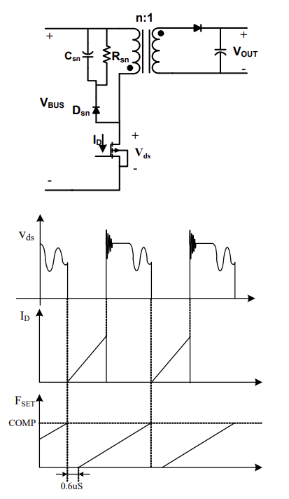
Figure 2: Key Waveforms of Off-Time Flyback Converter
Design Procedure
A. Predetermined Input and Output Specifications
- Input AC voltage range: Vac(min), Vac(max), for example 90Vac ~ 265Vac RMS
- DC bus voltage range: Vin(max), Vin(min).
- Output: Vo , Io(min), Io(max), Pout
- Estimated efficiency: η, It is used to estimate the power conversion efficiency to calculate the maximum input power. Generally, η is set to be 0.8~0.9 according to different output applications.
Then the maximum input power can be given as:
$$P_{in} = \frac {P_{out}}{η}$$Figure 3 shows the typical DC bus voltage waveform. The DC input capacitor Cin is usually set as 2μF/W for the universal input condition. For 230V single range application, the capacitance can be half the value.
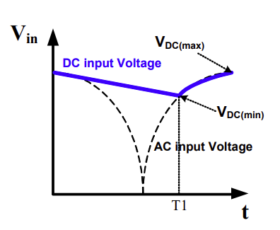
Figure 3: Input Voltage Waveform
From the waveform above, the AC input Voltage VAC and DC input Voltage VDC can be got as:
$$V_{DC}(V_{ac},t)=\sqrt{2 \times V_{ac}^2-\frac{2 \times P_{in}}{C_{in}}\times t}$$By setting VAC=VDC, T1 where DC bus voltage reaches to its minimum value VDC(min) can be calculated as
$$V_{DC(min)}=V_{DC}(V_{ac(min)},T1)$$Then, the minimum average DC input voltage Vin(min) can be got as:
$$V_{in(min)}=\frac{\sqrt{2}\times V_{AC(min)}+V_{DC(min)}}{2}$$The maximum average DC input voltage Vin(max) can be got as:
$$V_{in(max)}=\sqrt{2} \times V_{ac(max)}$$B. Determining the Startup Circuitry
Figure 3 shows the startup circuit. When power is on, the internal 2mA current source charges C1 through R1 connected to HV pin of HFC0300. Once VCC voltage reaches 11.7V, the internal high voltage current source (2mA) turns off and IC starts switching, then the auxiliary winding takes over the power supply. If VCC drops below 8.2V before the auxiliary winding takes over the power supply, the switching stops and the internal high voltage current source turns on again, which re-charges the VCC external capacitor C1, starting another start-up procedure(see Figure 4).
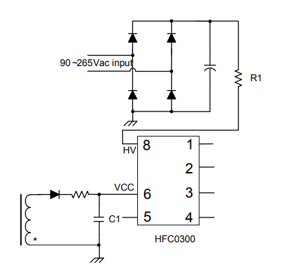
Figure 4: The Startup Circuit with HFC0300
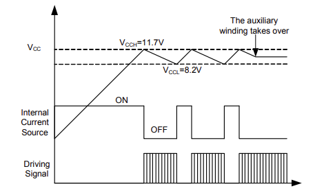
Figure 5: The Startup Waveform and VCC UVLO of HFC0300
C. Turns Ratio-N, Primary MOSFET and Secondary Rectifier Diode Selection
Figure 5 shows the typical voltage waveform of the primary MOSFET and secondary ectifier diode in a flyback converter. From the waveform, the primary MOSFET Drain-Source voltage rating Vds can be got as equation (6):
$$V_{ds}=\frac {Vin(max)+N\times(V_{out}+V_F)+60V}{k}$$Where k is the derating factor which is typically selected as 0.9. VF is the forward voltage of the rectifier diode, 60V spike voltage is assumed here.
The secondary rectifier diode voltage rating Vka can be estimated as equation (7):
$$V_{ka}=\frac {\frac{Vin(max)}{N}+V_{out}}{k}$$Where k is the derating factor which is typically selected as 0.9.
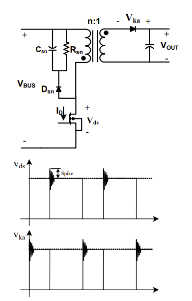
Figure 6: Voltage Stress of Primary MOSFET and Secondary Rectifier Diode
From equation (6) and (7), the voltage rating for primary MOSFET and secondary rectifier diode versus turns-ratio N can be calculated and shown in Figure 6.
For example, in 90Vac~265Vac input, 19V output adapter application, 650V MOSFET and 100V rectifier diode is preferred for better performance. From figure 7, N=6 is selected for the required voltage rating.
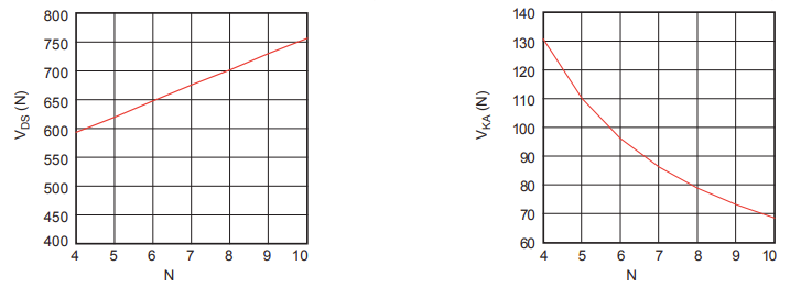
Figure 7: Voltage Stress Rating of Primary MOSFET and Secondary Rectifier Diode
D. Current Sense Resistor
The peak current level is internally set to be 0.5V, so current sense resistor sets the primary side peak current, which also determines the operation mode of the converter, such as CCM, BCM or DCM. If power supply is designed to operate at BCM at low line input, it will operate at DCM at high line and the same load condition. The magnetizing inductor current (reflected to the primary side) and the Drain-Source voltage of the primary MOSFET is shown as Figure 8.
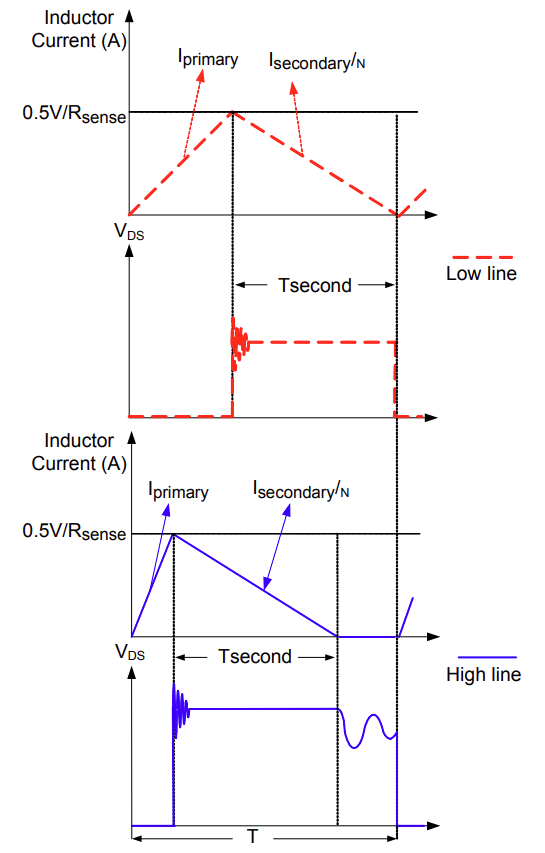
Figure 8: Inductor Current and Voltage of Primary MOSFET at Different Line
The time duration of secondary current can be got as equation (8).
$$T_{second}=\frac {L_m \times I_{peak}}{N \times V_O}$$Where Lm is primary magnetizing inductance, Ipeak is primary peak current. Since Ipeak is always the same at different input and same output conditions, so the time duration of secondary current is the same. The switching period can be calculated by equation (9).
$$T=\frac{N \times I_{peak} \times T_{second}}{2 \times I_o}$$From (9), the switching period also keeps the same at different input and same output conditions. Since the primary side switch on time decreases with the input voltage increasing, therefore, the higher the input line voltage, the deeper DCM mode it will enter. Usually, the parameters should be designed at the minimum input condition to guarantee the converter can deliver the required output power at minimum input condition.
Since N has been selected, so if the power supply is designed to operate at boundary current mode (BCM) at low line, the peak current can be calculated easily as equation (10).
$$I_{peak\_BCM}=\frac{2I_o}{1-D}$$Where D is the duty ratio of the switching, it can be got as equation (11).
$$D=\frac {(V_o+V_F)\times N}{V_{in}+(V_o+V_F)\times N}$$If the peak current set by current sense resistor is larger than Ipeak_BCM, the power supply will enter DCM. On the contrary, if the peak current set by current sense resistor is less than Ipeak_BCM, the power supply will enter CCM as Figure 9. Here, we define Kdepth as the depth of CCM.
$$K_{depth}=\frac{I_{valley}}{I_{peak}}$$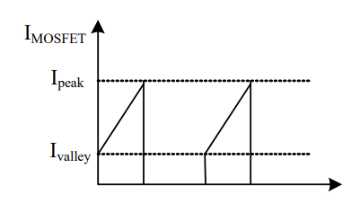
Figure 9: Primary Current at CCM
So peak current can be got as equation (13).
$$I_{peak}=\frac {2I_o}{(1-D)\times(1+K_{depth})\times N}$$Usually, BCM (boundary current mode) is preferred for the power level below 40W. CCM (continuous current mode) is selected when the power level is higher than 40W. The higher the power delivers, the deeper CCM should be adopted for higher efficiency and better thermal performance at full load. For example, for a 90W power supply, 0.5 could be chosen for Kdepth.
So when a power supply SPEC is given, we need to determine the converter operation mode firstly, i.e. determine the Kdepth. Ipeak and Ivalley can be calculated by equation (10) to (13). And the current sense resistor could be selected by equation (14).
$$R_{sense}=\frac{V_{peak}}{I_{peak}}$$Where Vpeak is the peak voltage threshold of the current resistor, it is a constant 0.5V for HFC0300. The current resistor with the proper power rating should be chosen based on the power loss given in equation (15)
$$P_{sense}=[(\frac{I_{peak}+I_{valley}}{2})^2+\frac{1}{12}(I_{peak}-I_{valley})^2]\times D \times R_{sense}$$E. Primary side Inductance Lm
The power that a flyback converter can deliver is related to the energy stored in the primary side inductance Lm as given in equation (16) and (17) for CCM and DCM respectively.
$$\frac {1}{2} \times L_m \times (I_{peak}^2 - I_{valley}^2) \times f_s = \frac {p_{o\_CCM}}{η}$$ $$\frac {1}{2} \times L_m \times I_{peak}^2 \times f_s = \frac {p_{o\_CCM}}{η}$$In order to regulate the delivered power to the output, we can either adjust the peak current value (conventional peak current mode control) and/or adjust the switching frequency. HFC0300 regulates the output power by adjusting the switching frequency while keeping the peak current value constant. Thus, once the peak current is selected, the feedback loop automatically sets the switching frequency to get the desired output power.
Since Ipeak and Ivalley have been determined at the beginning of the design procedure, Lm can be calculated if fs is chosen. Offering a good EMI performance, a maximum frequency of 65kHz is usually a good choice because the conducted EMI noise at second harmonics (2*65kHz) is still not tested (conducted EMI frequency range:150kHz~30MHz)
As mentioned in section D, the switching frequency keeps the same ideally at different input line voltage and the same output power. Actually, there is slightly difference in the practical circuit. Since the peak current will be a little bit higher at high input than that at low input due to the inevitable propagation delay though the threshold is constant, the switching frequency will reaches its maximum at low line and full load condition. So we usually choose 65kHz as the frequency at low line and full load. As a result, all the calculation is carried at lowest line.
F. Design of CFSET and OLP function
The maximum frequency is set by the end of charge of the capacitor CFSET connected to the FSET pin as shown in Fig 10. This capacitor is charged by a constant current source shortly after the primary side switch turns on (about 0.6us), and its voltage is compared with COMP voltage from feedback loop (see Figure 10). When this capacitor voltage reaches the threshold, the capacitor is rapidly discharged down to 0V, and a new period starts. To make the voltage at FSET pin fully discharged, it is internally about 0.6μs delay before the CFSET is charged again (see Figure 11). Thus the switching frequency is regulated by the feedback loop like a VCO (voltage controlled oscillation). The capacitance connected to FSET pin is got as equation (18).
$$C_{FSET} = \frac {28uA \times (\frac {1}{f_{max}}+0.6us)}{0.88V}$$Where fmax is the maximum frequency set by the capacitor connected to FSET pin.
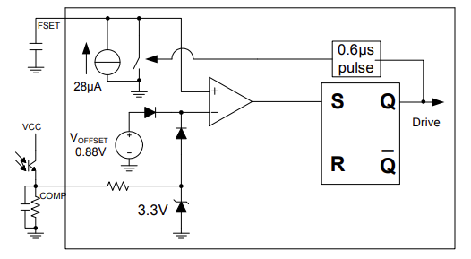
Figure 10: VCO (Voltage Controlled Oscillation) Operation

Figure 11: COMP Voltage adjusts the Switching Frequency
As described as above section, the switching frequency reaches its maximum at low line and full load. We define this frequency as fs( 65kHz selected here). We set maximum frequency (fmax) as about 110% fs. Frequency increases with the increasing of the output power. When the frequency reaches maximum frequency which is set by CFSET, over power limitation takes place which makes output voltage can’t be maintained, thus COMP is saturated and below OLP (over load protection) threshold (0.85V).
A unique digital timer method is employed in HFC0300 for over load protection (OLP). When COMP is lower than 0.85V which is considered as an error flag, the timer starts counting. If the error flag removes, the timer resets. If the timer overflows when the counting number reaches 6000, OLP will be triggered. This timer duration avoids triggering OLP function when the power supply is at start up or load transition phase. So output voltage should be established in less than 6000 switching cycles during startup.
_______________________
Did you find this interesting? Get valuable resources straight to your inbox - sent out once per month!
Technical Forum
 Latest activity a day ago
 3 Comments
Latest activity 5 days ago
2 Comments
Latest activity 3 weeks ago
3 Comments
3 Comments
Latest activity 5 days ago
2 Comments
Latest activity 3 weeks ago
3 Comments
Log in to your account
Create New Account