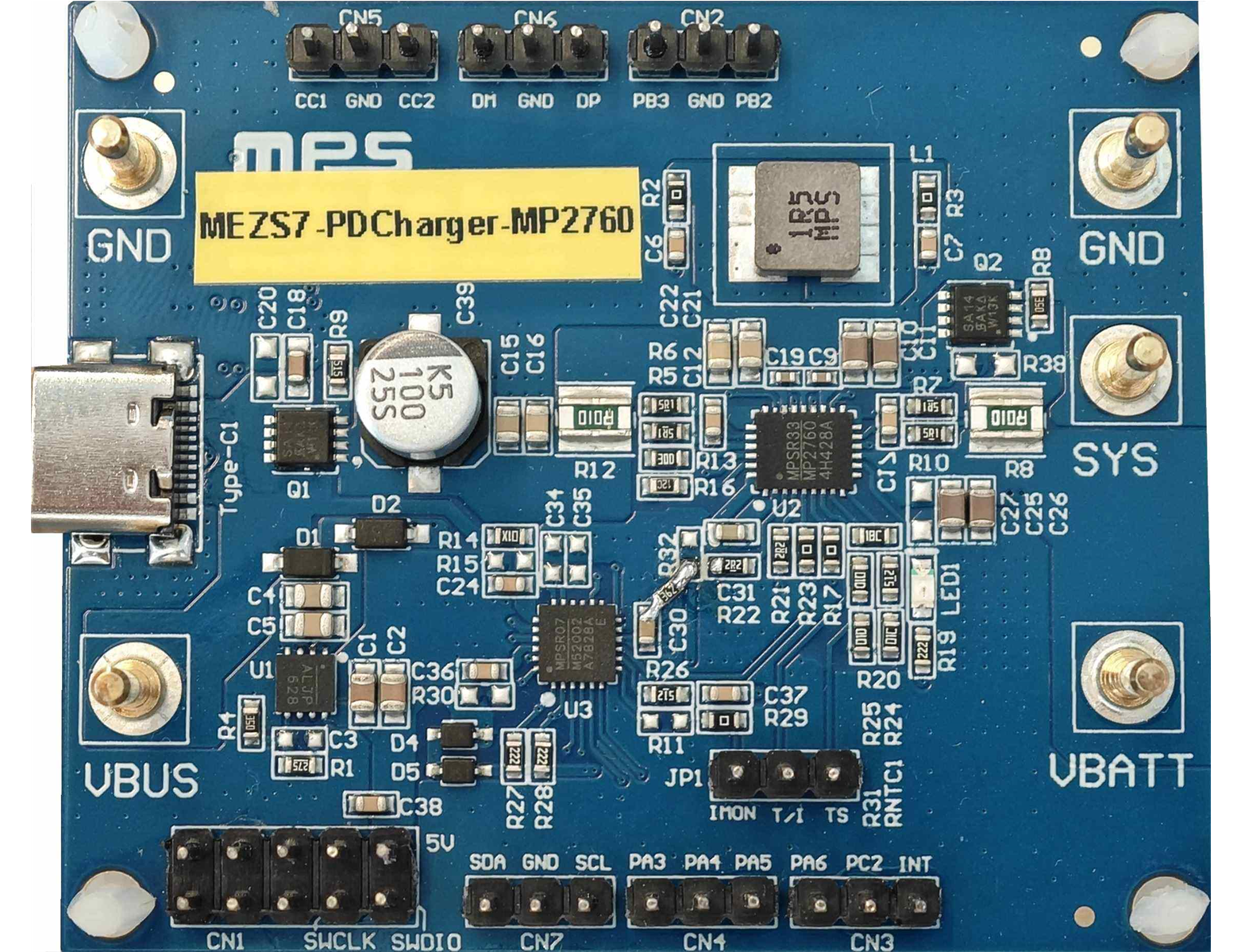
MEZS7-PDCharger-MP2760 Reference Design
DOWNLOAD THE FULL REFERENCE DESIGN

Get valuable resources straight to your inbox - sent out once per month
We value your privacy
Description
The MEZS7-PDCharger-MP2760 is a solution module for dual-role port (DRP) applications using the MP2760 and MPF52002.
The MP2760 is a 4V to 22V input voltage (VIN) buck-boost charger IC designed for battery packs with 1 to 4 cells in series. It also supplies a wide voltage range (5V to 21V) at the IN pin in source mode, which is compliant with USB power delivery (PD). It also has an output current limit with a high resolution in source mode.
The MPF52002 is a highly integrated USB PD controller for DRP ports, with a 32-bit ARM Cortex-M0 microcontroller (MCU). It supports automatic DRP toggling for DRP applications, and it is compliant with PD3.1 specifications. For source mode, the MPF52002 supports PD3.1, as well as BC1.2, Apple divider mode, Huawei FCP/SCP, and QC2.0/3.0.
The MEZS7-PDCharger-MP2760 contains a DRP USB Type-C port, supporting PD3.1 and BC1.2 protocols. When an adapter is inserted, the port acts as a sink port to charge the battery with a maximum 6A charge current. When a load is inserted, the port acts as a source port to power the USB VBUS from the battery.
Performance Summary (1)
Specifications are at TA = 25°C, unless otherwise noted.
| Parameters | Conditions | Default Value |
| Sink Mode | ||
| Input voltage (VIN) range | 4V to 22V | |
| Input current(IIN) limit | Up to 5A | |
| Battery charge regulation voltage (VBATT_REG) (2) | 8.4V | |
| Fast charge current (2) | VIN = 9V to 20V | 3A |
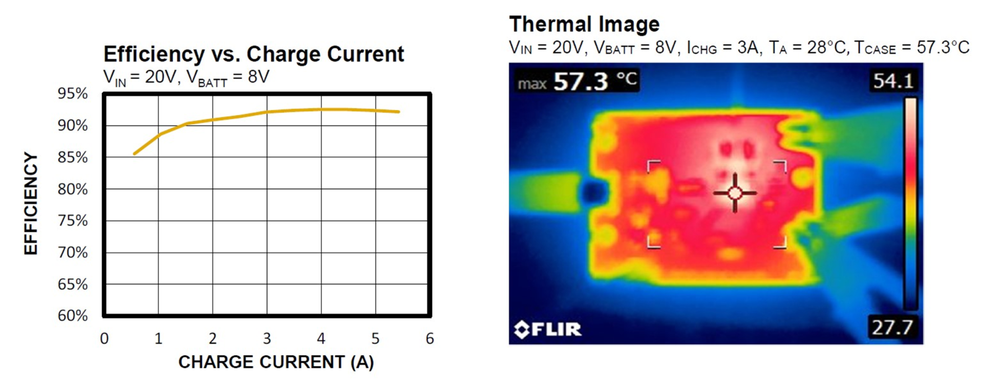
| Charge typical efficiency | VIN = 20V, VBATT = 8V, ICC = 3A |
92.2% |
| Source Mode | ||
| Battery voltage range | Up to 18.72V | |
| Output voltage in source mode (VIN_SRC) (3) | 5V to 21V | |
| Default PDO output | 5V/3A, 9V/3A, 15V/1.8A, 20V/1.35A, 5V to 5.9V/3A, 5V to 11V/3A, 5V to 16V/1.8A | |
| Source mode typical efficiency | VBATT = 8V, VIN_SRC = 9V, IIN_SRC = 2.6A | 93.6% |
1) Refer to the MP2760 datasheet for more details.
2) These items can be configured by the MPF52002 via the I2C interface.
3) These items are configured by the MPF52002 automatically, according to the protocol.
Evaluation Board
LxWxH (6cmx5cmx2.1cm)
| Board Number | MPS IC Number |
| MEZS7-PDCharger-MP2760 | MPF52002GRE-001C |
| MP2760GVT-000A |
Table 1: Battery Cell Number and VSYS_MIN Setting (4)
| Cell Number | VSYS_MIN | PB2 | PB3 |
| 2-Cell (Default) | 6.2V | 1: Float or high | 1: Float or high |
| 3-Cell | 9V | 0: Short to GND | 1: Float or high |
| 4-Cell | 12V | 1: Float or high | 0: Short to GND |
4) Set PB2 and PB3 to configure the cell number and VSYS_MIN before charging a real battery.
Quick Start Guide
The MEZS7-PDCharger-MP2760 is a 2-cell to 4-cell series power delivery (PD) charger module using the MP2760 and MPF52002. It is a reference design for PD applications and includes a DRP USB Type-C port. The charge current is preset to 3A, and the charge-full voltage is preset to 8.4V for a 2-cell series Li-ion battery. In reverse source mode, the output is preset to 5V/3A or 27W PD. All the charging/discharging parameters are set by the MPF52002.
The user can download their own charge parameter settings to the MPF52002’s volatile memory via the I2C after start-up. The user can also download these parameters to the MPF52002’s non-volatile memory (NVM), which is not reset until even if the part completely powers off.
Follow the steps below to prepare the battery and load connection for testing:
- Connect the series battery terminals to:
- Positive (+): VBATT
- Negative (-): GND
- Positive (+): VBATT
- Negative (-): GND
- Ensure that the battery voltage is present (if using a battery simulator, keep the simulator on).
- Connect the system load terminals to:
- Positive (+): SYS
- Negative (-): GND
If using a battery simulator, preset the battery voltage, then turn it off. Connect the battery simulator output terminals to:
Before adapter plug-in, ensure that the PB2 and PB3 settings are correct (see Table 1). Otherwise, the system load and battery may be damaged.
Sink Mode
Connect the USB Type-C port to an adapter with a USB Type-C to Type-C or Type-A to Type-C cable. MP2760’s IIN_LIM and adapter’s output voltage is set according to the negotiation result between the adapter and board, and then charger operation starts.
The default firmware of the MPF52002 on this evaluation board supports the following protocols in sink mode:
- PD3.1
- For a non-PD adapter, the bus voltage (VBUS) is 5V. The default input current (IIN) limit is 900mA. If there is a Rp on source CC termination, then IIN_LIM can rise to 1.5A or 3A, according to the Rp value.
The MPF52002 automatically requests the maximum input power, according to the adapter’s protocol.
The MPF52002 sends an I2C command to the MP2760, and then MP2760 charges the battery. For 2-cell applications, the default minimum system voltage (VSYS_MIN) is 6.2V, and the default battery-full regulation voltage is 8.4V. The CC charge current limit is set to 3A by default.
If the input power is sufficiently high, the charge current is 3A by default. The real charge current may be limited by the input power limit if the input power is not sufficiently high. If the maximum adapter power is below the maximum charging power rating, the input current limit loop adjusts the charge current to avoid overloading the source/adapter.
Figure 1 shows the set-up for sink mode.
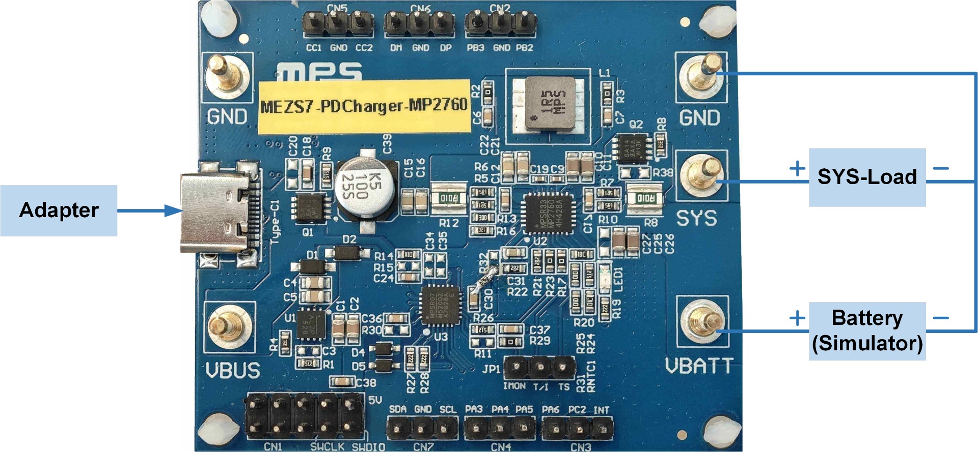
Figure 1: Sink Mode Set-Up
Source Mode
Connect the devices to the USB Type-C port with a USB Type-C to Type-C, Type-C to micro-B, or Type-C to lighting cable. Source mode can start automatically and provide the proper voltage to devices as requested.
The default firmware for the MPF52002 on this evaluation board supports the following protocols in source mode:
- PD3.1
- DCP
- Apple mode
VBUS should start up automatically at the default voltage set by the PD protocol sniffer or mobile device. The PD protocol sniffer can select different PDO outputs.
The default PD output power is 27W.The battery discharge current limit is 6.4A.
Figure 2 shows the set-up for source mode.
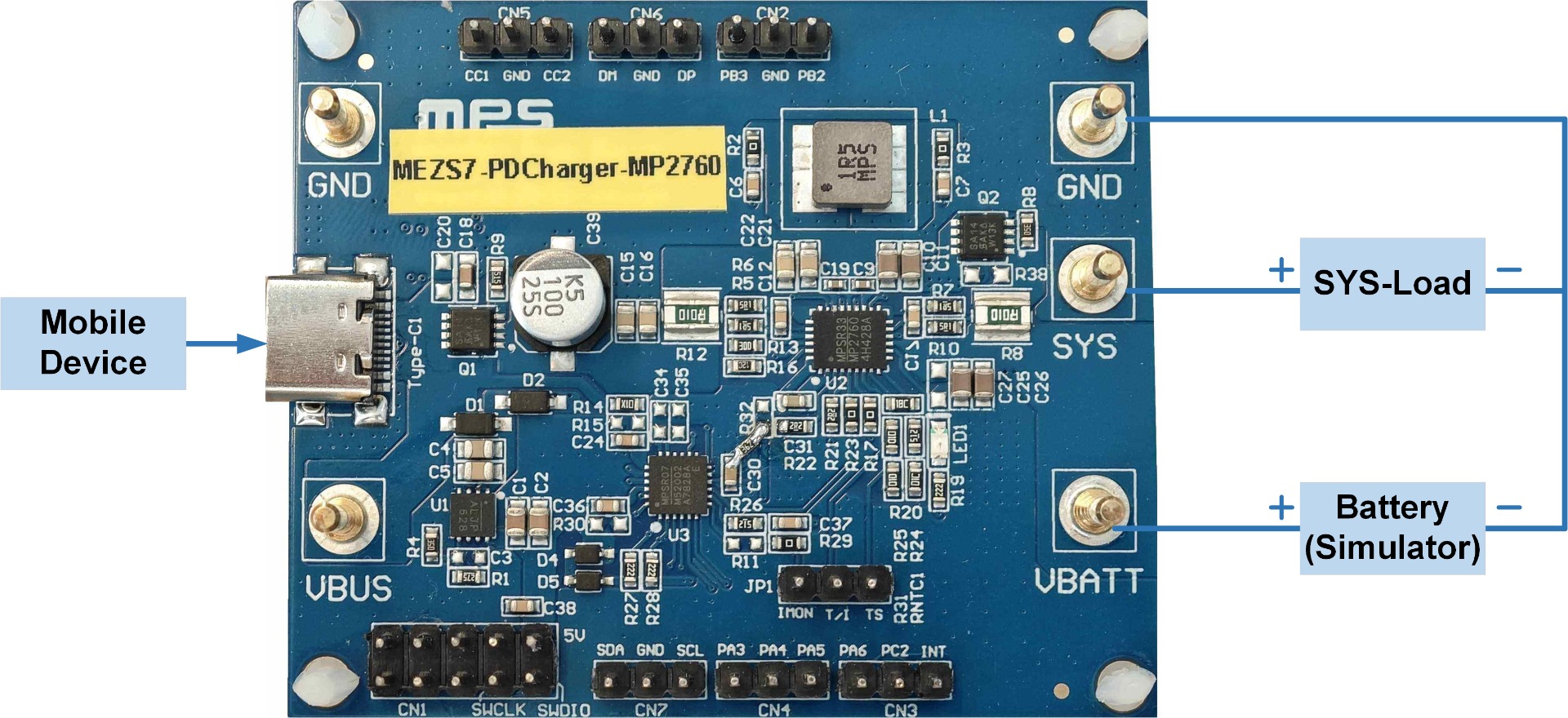
Figure 2: Source Mode Set-Up
I2C Target Function Description
The MP2760 and MPF52002 can be controlled or monitored via the I2C between the MPF52002 and I2C initiator (see Figure 3). The initiator should be connected to the MPF52002 through the I2C (PB6 and PB7) instead of the MP2760. The MPF52002 periodically reads the MP2760’s charge parameters and alert status, then updates the information to the I2C target registers. The initiator can also send certain I2C commands to the MP2760 through the MPF52002.
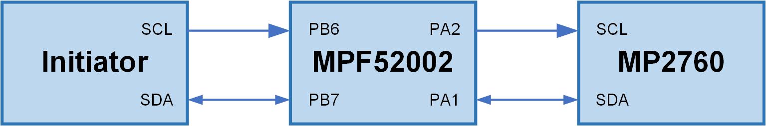
Figure 3: MPF52002 I2C Target Diagram Block
Hardware Set-Up for I2C Connection
The MPF52002 enters a deep sleep status to save power when the device is only using a battery, and I2C target is disabled. Before starting I2C communication, there are two methods to make the MPF52002 and I2C target function wake up, described below.
- Short PB1 (INT pin in CN3) to GND in battery-only mode.
- A USB Type-C device or adapter is connected to the USB Type-C port.
After communication wakes up, connect the PC and evaluation board with dongle(the EVKT-USBI2C-02 communication interface). The I2C’s SCL should be connected on PB6, which has a SWDIO silkscreen print. The I2C’s SDA should be connected on PB7, which has a SWCLK silkscreen print (see Figure 4).
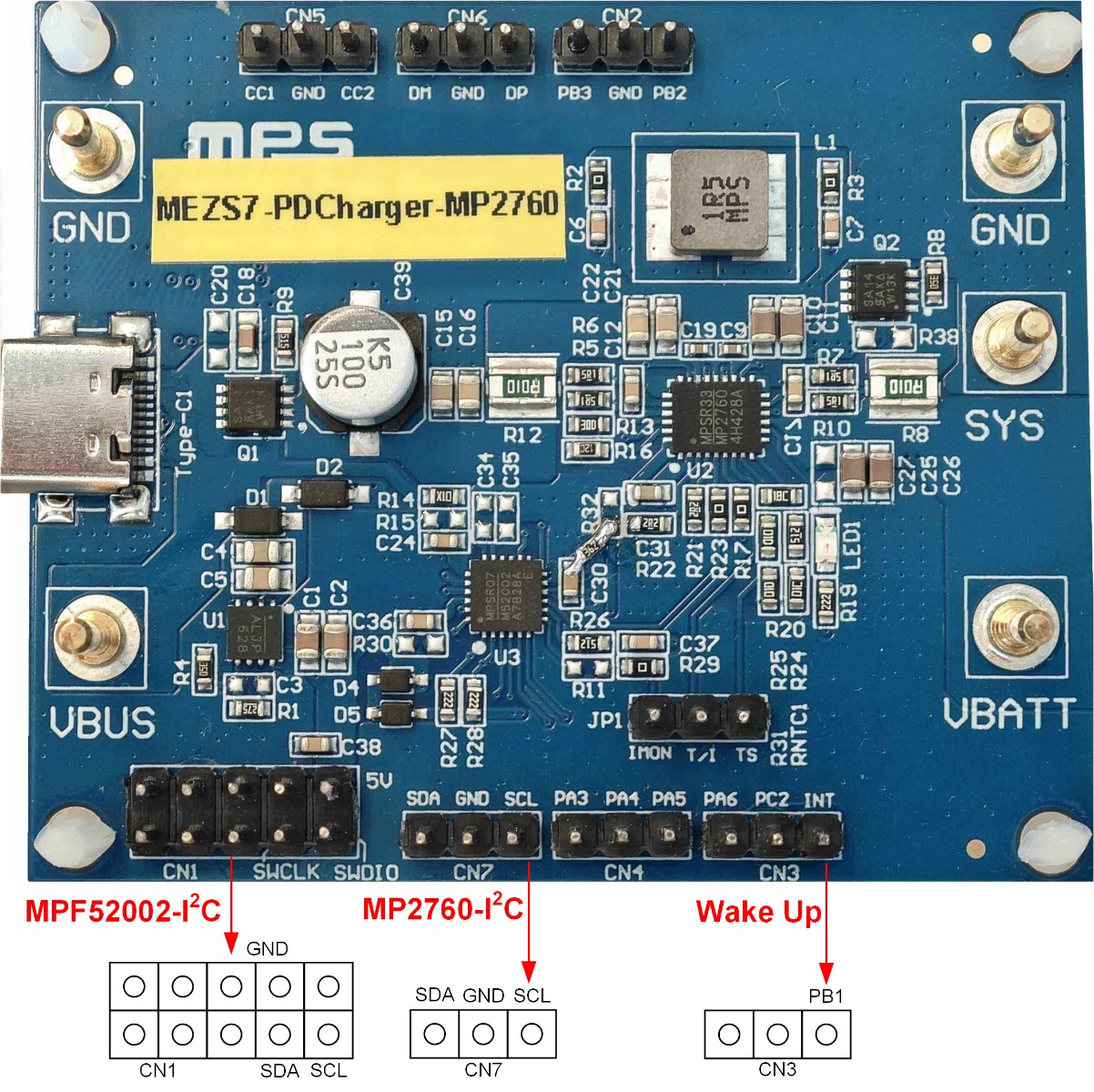
Figure 4: Hardware Connection for I2C Communication
Time Requirements for the I2C Initiator
- The initiator SCL clock frequency is 400kHz (fast mode), compliant with a 100kHz to 400kHz clock.
- Read or write 1 byte in every command. Does not support reading/writing multiple bytes.
- A 10ms (or longer) delay between two I2C commands is recommended.
Evaluation Board Schematic
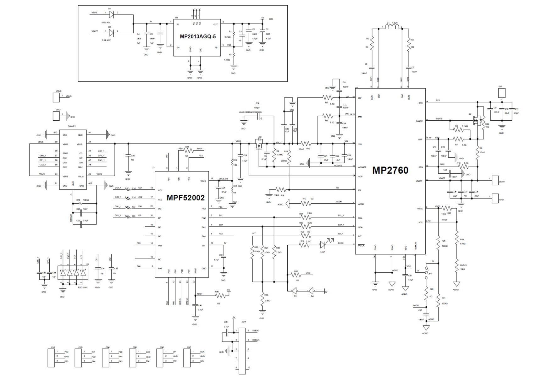
Figure 5: Evaluation Board Schematic
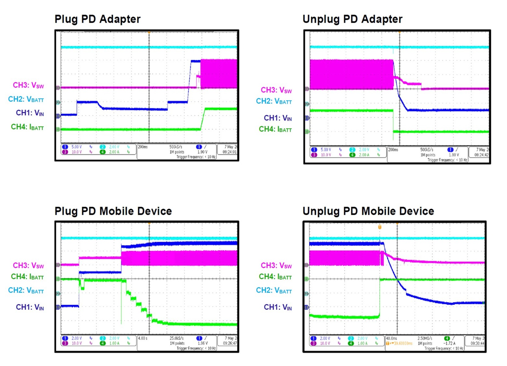
Solution Module Test Results
Performance curves and waveforms are tested on the evaluation board. The input power source is a PD adapter, VIN = 20V, VBATT = 8V, TA = 25°C, default register data, unless otherwise noted.
Log in to your account
Create New Account