Working Principles for Selecting a Boost Converter

Get valuable resources straight to your inbox - sent out once per month
We value your privacy
Introduction
Converter selection is the first step in power supply design that directly impacts stable system operation and performance. Typically, the designer must determine whether a power converter meets the actual load capacity based on the rated current value.
For example, selecting a 36V/3A buck converter for a 24V to 5V/2A power rail achieves excellent efficiency, temperature rise, and cost performance. However, if a 3A/5.5V boost converter is selected for a 3.6V to 5V/2A power rail, then the chip protection mechanism is triggered abruptly. This is because the boost converter’s nominal current is not equivalent to the amount of current that the converter can output.
This article discusses the working principles of the boost converter to determine the switching current capability.
Boost Converter Working Principles
When the switch tube (M1) turns on within one switching cycle, the current path occurs in the following order: input voltage (VIN), inductance (L), and M1. The inductor current (IL) rises, resulting in energy storage in the inductor (see Figure 1).
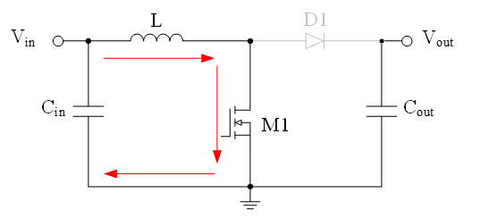
Figure 1: Current Path when M1 Turns On
Related Content
-
ARTICLE

Understanding Quiescent Current and Shutdown Current with a Boost Converter
Learn the difference between a boost converter’s IQ and shutdown current (ISD) to provide a deeper understanding of how IQ and ISD can be utilized in battery-powered applications
-
VIDEO

Feasibility and Accuracy Analysis of Input Power Estimation for Boost PFC Converter without Additional Sensor
This presentation discusses the feasibility of estimating real-time input power based on this limited information in a boost converter, using the HR1211 as an example
-
VIDEO

Understanding Power over Ethernet and PoE Controllers and Converters
Explore what power over ethernet (PoE) means for your design
-
ARTICLE

PCB Design for Low-EMI DC/DC Converters
The MPQ4431 buck converter demonstrates that careful component placement and board layout help make it possible to meet the strict EMC limits within the automotive industry
When M1 turns off, the diode (D1) continues to flow and the inductor releases energy since IL does not change abruptly. The current path occurs in the following order: VIN, L, D1, and output voltage (VOUT) (see Figure 2).
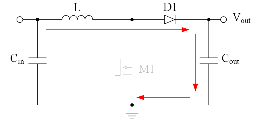
Figure 2: Current Path when M1 Turns Off
In the boost circuit during a switching cycle, the input continuously transfers energy to the output through the inductor’s energy storage and release (see Figure 3).
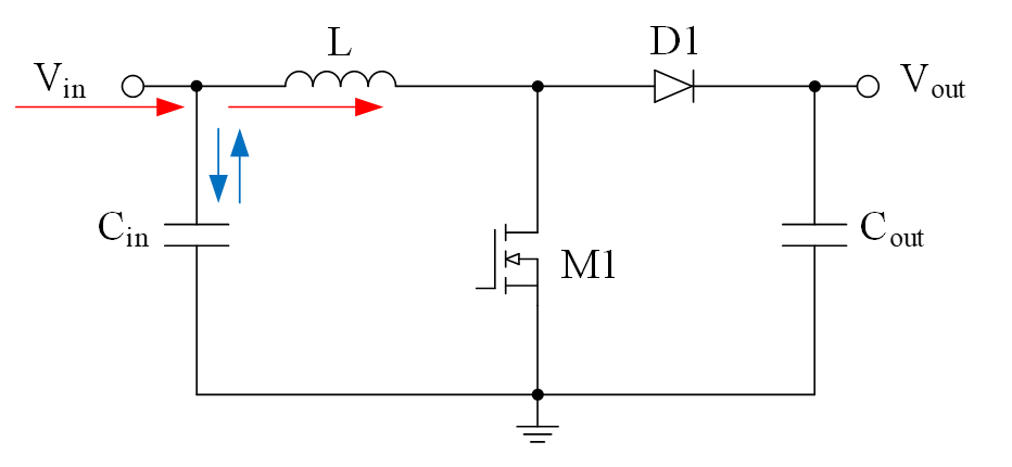
Figure 3: Continuous Energy Transfer to the Boost Circuit Output
Due to the charging and discharging balance of the input capacitor during a cycle, the average current is 0A. Therefore, the average IL is equal to the average input current (IIN_AVG), and the maximum IL is equal to the maximum switch current (see Figure 4).
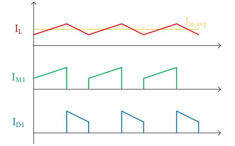
Figure 4: Inductor Current, Switch Tube Current, and Diode Current Waveforms
The nominal current of buck converters is IOUT, while the nominal current of boost converters is the maximum switching current. The maximum switching current is equal to the peak inductor current (IL_PEAK). Due to the ripple in IL, IL_PEAK must be calculated with Equation (1):
$$I_{L\_PEAK}=(\frac {V_{OUT}\timesI_{OUT}}{V_{IN\_MIN}\times\eta})\times1.15$$Calculate the maximum output power (POUT_MAX) using VOUT and IOUT. Divide VOUT and IOUT by efficiency η to obtain the maximum input power (PIN_MAX), then divide PIN_MAX by the minimum VIN to determine the maximum input current (IIN_MAX).
Where the current is the average value. Multiply the average current by the current ripple coefficient to obtain the peak-to-peak IL value.
The ripple coefficient is typically 30%, meaning IL_PEAK is equal to the average current multiplied by 1.15 times. According to this formula, IL_PEAK must be below the maximum current flowing through the switch tube to make a preliminary selection of the chip (see Figure 5).
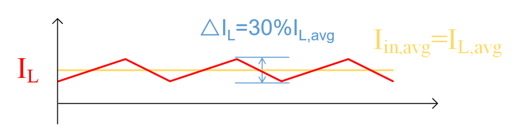
Figure 5: Peak Inductor Current for Preliminary Chip Selection
Conclusion
This article discusses the steps for determining the switching current capability for boost converters, which combined with VIN and VOUT requirements, are necessary for proper boost converter selection. For more details, explore MPS’s wide selection of boost controllers and converters.
_______________________
Did you find this interesting? Get valuable resources straight to your inbox - sent out once per month!
Technical Forum
 Latest activity 8 hours ago
 1 Comment
Latest activity 21 hours ago
3 Comments
Latest activity a day ago
1 Comment
1 Comment
Latest activity 21 hours ago
3 Comments
Latest activity a day ago
1 Comment
Log in to your account
Create New Account