Selecting the Switching Frequency in Automotive Applications

Get valuable resources straight to your inbox - sent out once per month
We value your privacy
Introduction
This article will discuss the key factors in the energy conversion process, then analyze automotive applications at three switching frequency (fSW) levels: 2MHz, 100kHz, and 500kHz.
Energy Conversion Process
In a buck circuit, the energy conversion process includes the input capacitance (CIN), output capacitance (COUT), the energy stored in the inductor, and fSW. fSW can impact the following factors: device size, efficiency, temperature rise, and the minimum turn-on and minimum time-off times.
Device Size
The relationship between device size and fSW can be determined using CIN, COUT, and the energy stored in the inductor. As fSW rises, less capacitance and inductance are required, which reduces device size. Figure 1 shows the required peripheral device parameters that can be obtained for 12V to 3.3V operating conditions at 2A.

Figure 1: Required Peripheral Device Parameters
Switching Loss and Temperature Rise
Under the same operation conditions from Figure 1, the efficiency curves at different frequencies were obtained (see Figure 2). These parameters are useful because they allow designers to determine the device’s temperature rise, where lower efficiency results in a higher temperature rise.
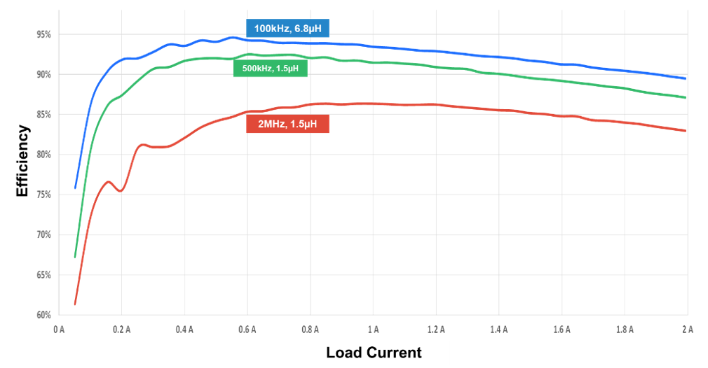
Figure 2: Efficiency Curves at Different Frequencies
Minimum On and Off Time Limit
If the input voltage (VIN) increases, the chip’s switching on time decreases. In this situation, decreasing fSW can avoid triggering the device’s minimum on time (tON_MIN). If VIN decreases, the chip’s switching off time decreases. In this situation, decreasing fSW can avoid triggering the device’s minimum off time (tOFF_MIN).
Selecting the Switching Frequency
We will analyze performance at three different fSW levels (100kHz, 500kHz, and 2MHz) to determine how these frequencies affect automotive applications. To accommodate varying fSW levels, fSW was set to be below 300kHz, between 300kHz and 530kHz, or above 1.8MHz.
- 100kHz: Automotive applications can achieve excellent efficiency at this frequency with low switching loss. At 100kHz, application can achieve stable operation at an ambient temperature of 85°C with greatly reduced heat generation. However, this frequency is not recommended for space-constrained applications.
- 500kHz: Most automotive USB charging and LED lighting applications operate at 500kHz because it optimizes the tradeoff between efficiency and solution size.
- 2MHz: At 2MHz does not generate significant EMI in the AM frequency band. However, this frequency may exacerbate EMI in the high frequency band.
fSW selection is important to manage EMI for DC/DC converters in automotive applications. Figure 3 shows a standard limit chart for CISPR25 Class 3 CE. The three fSW levels (100kHz, 500kHz, and 2MHz) fall within these three intermittent regions.
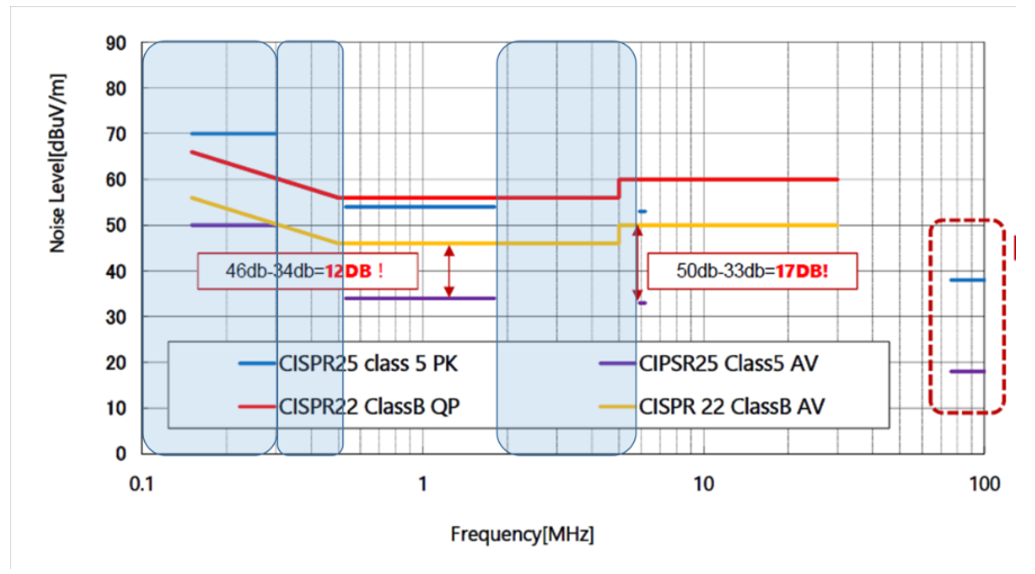
Figure 3: CISPR25 Class 3 CE Limit Standard Chart
The next step is to evaluate the three fSW levels in different applications and select the required fSW using three application examples: onboard camera sensors, onboard mobile charging devices, and autonomous driving controllers.
Onboard Camera Sensors
Figure 4 shows a diagram of an onboard camera sensor.
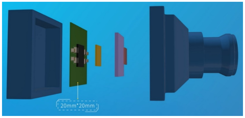
Figure 4: Onboard Camera Sensor
Onboard sensors are typically made to be as small as possible, which means the peripheral components (e.g. inductors and capacitors) should also be small. For switching power supplies, fSW must be high to ensure that the inductors and capacitors can stay small. For space-constrained applications, setting fSW to 2MHz is recommended because it mitigates EMI issues while minimizing heat generation and the camera’s power consumption.
For a 12V input, the current is generally between 100mA and 200mA, leading to a relatively small conduction loss for the DC/DC converter. Therefore, even if fSW increases, the higher switching loss does not produce a significant temperature rise for the power supply. At the same time, the camera module’s overall power consumption is minimized. The power supply here is a highly integrated power management IC (PMIC) solution. These factors optimize the high-frequency dI/dt loop and improve EMI performance.
Setting fSW to 2MHz ensures that a small solution can obtain excellent efficiency and EMI performance.
Onboard Mobile Charging Devices
Figure 5 shows onboard USB charging.
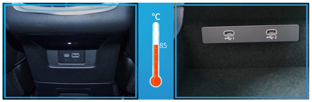
Figure 5: Onboard USB Charging
USB charging started from the original single-port USB Type-A, which was updated to the dual-port USB Type-A. Dual-port USB Type-C followed, leading up to the current USB Type-C power delivery (PD) ports. These charging devices have size requirements for the PCB board. Unlike camera modules though, the product is typically constrained at about 50mmx50mm.
If the PCB board size is also limited by the layout and device size, the 2MHz fSW level is not an optimal solution. Consider a dual-port USB Type-C where each charging port can reach 5V at 3A. The total power reaches 30W, and even considering the 94% efficiency, there is still about 2W of heat on the PCB board. Testing in onboard automotive environments typically considers stable operation at 85°C.
Considering the factors of power consumption and size, the 500kHz fSW level is the most suitable fSW option for onboard mobile device chargers.
Autonomous Driving Controllers
Figure 6 shows a 360-degree surround view electronic control unit (ECU).
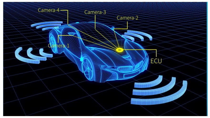
Figure 6: 360-Degree Surround View ECU
For autonomous driving controllers, the board area has more space. Compared to camera modules and USB charging, an autonomous driving controller has sufficient PCB layout area and space for heat dissipation. As a result, fSW selection is not as strict, but the chip’s the tON and tOFF limits must be considered.
For example, in a commercial vehicle, the battery system is 24V and the highest steady-state voltage reaches 32V. In a 360-degree surround view system, a 3.3V power supply is typically required, leading to a large voltage difference. If fSW is set to 2MHz, the on time (tON) can be calculated with Equation (1):
$$T_{ON}=\frac{3.3V}{32V} \times \frac{1}{2.0MHz}\approx 51ns$$Figure 7 shows the specifications of the MPQ4323-AEC1’s minimum on time (tON_MIN). For this application, a lower frequency must be selected to avoid triggering tON_MIN.

Figure 7: Minimum On Time Specifications
Occasionally, an 8V power rail is provided in the surround view system to act as the camera module’s input power. Assuming a 12V battery system for passenger cars, it is often necessary to consider the 9V to 16V VIN operating range with operating conditions at VIN = 9V and VOUT = 8V. If the 2MHz fSW level is selected, the off time (tOFF) can be calculated with Equation (2):
$$T_{OFF}=(1-\frac{8V}{9V})\times \frac{1}{2.0MHz}\approx 55.6ns$$Figure 8 shows the specifications of the minimum off time (tOFF_MIN). The maximum time is 70ns, meaning tOFF_MIN would be triggered.

Figure 8: Minimum Off Time Specifications
To ensure the chip’s stable operation at a set fSW, it is necessary to select the optimal fSW based on specific VIN and output voltage (VOUT) conditions.
Conclusion
This article reviewed the overall energy conversion process and discussed the different characteristics of three fSW levels (2MHz, 100kHz, and 500kHz). Using application examples with onboard sensors, onboard mobile charging devices, and autonomous driving controllers, we obtained the most suitable fSW levels that achieve stable switching power supply performance.
For more information, refer to MPS’s ADAS and Infotainment applications.
_______________________
Did you find this interesting? Get valuable resources straight to your inbox - sent out once per month!
Technical Forum
 Latest activity 7 days ago
 3 Comments
Latest activity 2 weeks ago
2 Comments
Latest activity 4 weeks ago
4 Comments
3 Comments
Latest activity 2 weeks ago
2 Comments
Latest activity 4 weeks ago
4 Comments
Log in to your account
Create New Account