Understanding LLC Operation (Part I): Power Switches and Resonant Tank

Get valuable resources straight to your inbox - sent out once per month
We value your privacy
Introduction
LLC resonant converters have become a hot topic in power electronics because they can meet the demanding performance requirements set by modern power supply designs. The LLC is one of a significantly larger family of resonant converter topologies, all of which are based on resonant tanks. Resonant tanks are circuits made up of inductors and capacitors that oscillate at a specific frequency, called the resonant frequency.
Because they allow for higher switching frequencies (fSW) and reduce switching losses, these switch-mode DC/DC power converters are often used in high-power, high-efficiency applications. LLC resonant converters are ideal for power supply applications with delicate systems (i.e. high-end consumer electronics), or power-demanding operations (i.e. charging electric vehicles).
An LLC converter is made up of 4 blocks: the power switches, resonant tank, transformer, and diode rectifier (see Figure 1). First, the MOSFET power switches convert the input DC voltage into a high-frequency square wave. This square wave then enters the resonant tank, which eliminates the square wave’s harmonics and outputs a sine wave of the fundamental frequency. The sine wave is transferred to the secondary of the converter through a high-frequency transformer, which scales the voltage up or down, according to the application. Lastly, the diode rectifier converts the sine wave into a stable DC output.
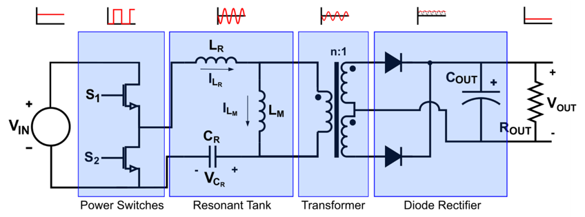
Figure 1: Circuit Schematic of a Simplified LLC Converter
The LLC converter’s ability to maintain high efficiency even at very high power comes from its resonant nature. The resonant nature of LLC converters enable soft switching in both the primary and secondary sides, increasing efficiency by reducing switching losses.
In addition, an LLC topology saves board space. LLC topologies do not have an output inductor, which means that all inductors can be more easily integrated into a single magnetic structure to save area and cost. When all of a circuit’s inductive elements are placed in the same structure, electromagnetic compatibility is improved, since it is easier and cheaper to shield one structure than three.
Power Switches
The power switches can be implemented in full-bridge or half-bridge topologies, and each has a unique output waveform (see Figure 2).
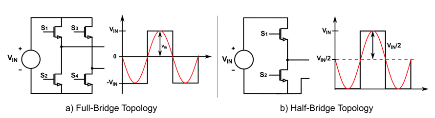
Figure 2: Power Switch Topologies
The main difference between these topologies is that full-bridge topologies generate a square wave with no DC offset, and an amplitude equal to the input voltage (VIN). Half-bridge topologies emit a square wave that is offset by (VIN / 2), and thus has half the amplitude of the full bridge wave.
Each topology has its own set of benefits and drawbacks. A full-bridge topology requires more transistors, which makes its implementation more expensive. Moreover, the added transistors incur an increased series resistance (RDS(ON)), which can increase conduction loss. On the other hand, a full-bridge implementation reduces the necessary transformer turn ratio (N) by half, which minimizes the copper loss in the transformer.
A half-bridge topology is more cost-effective to implement and has the added benefit of reducing the RMS current across the capacitor by approximately 15%, but it also increases switching loss.
Considering these trade-offs, it is recommended to use a half-bridge power switch topology for applications where the power is below 1kW, and a full-bridge topology for applications with higher power.
Related Content
-
VIDEO
Feasibility and Accuracy Analysis of Input Power Estimation for Boost PFC Converter without Additional Sensor
Accurately estimate input power for your design
-
ARTICLE

Digital PFC + LLC Combo Controller Helps Fast-Charge Adapters Enter the New Age
Discover our digital PFC + LLC controller solutions
-
VIDEO

Multi-Mode PFC and Current Mode LLC 2-in-1 Controller: HR1211
Power-saving technology optimizes efficiency
-
REFERENCE DESIGN

Offline 600W Battery Charger: PFC + LLC with HR1211
Learn more about the EVHR1211-Y-00B
Resonant Tank
The resonant tank is made up of a resonant capacitor (CR) and two inductors: the resonant inductor (LR), in series with the capacitor and transformer, and the magnetizing inductor (LM), in parallel. The tank’s role is to filter out the square wave’s harmonics, outputting a sine wave of the fundamental switching frequency to the input of the transformer.
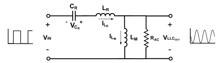
Figure 3: Schematic of an LLC Tank with a Primary-Referenced Load
The resonant tank has a gain that varies according to the frequency and the load applied to the secondary side (see Figure 4). Designers must tune these parameters to ensure that the converter efficiently operates across a wide range of loads by designing the tank’s gain to exceed 1 for all load values.
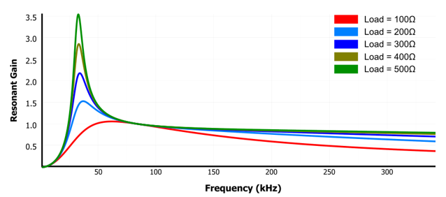
Figure 4: Resonant Gain Response across A Range of Loads
The LLC converter has a wide operation range and high efficiency due to the resonant tank’s dual inductors. To understand how this works, consider the tank’s response to heavy and light loads, depending on the inductor.
Figure 5 shows the resonant tank’s gain for a range of loads if the resonant tank were only composed of the resonant capacitor and the magnetizing inductor. At light loads, there is a clear peak in the resonant tank’s gain. However, the gain for the heavy load does not peak — instead, it has a dampened response and only achieves unity gain at very high frequencies.
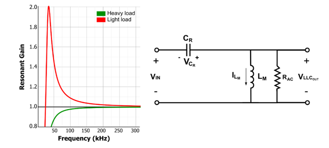
Figure 5: Gain Response and Schematic for an LC Tank with Parallel Inductor
If the resonant tank is only made up of the resonant inductor (LR) in series with the resonant capacitor, the behavior is different. The gain does not exceed 1, but when the load is heaviest, the tank reaches unity gain much more quickly than it would with the parallel inductor.
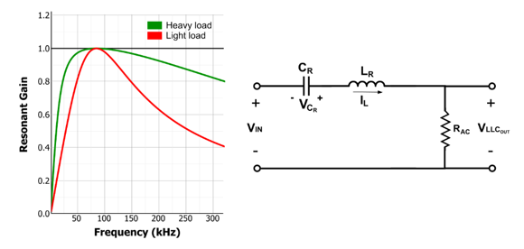
Figure 6: Gain Response and Schematic for an LC Tank with a Series Inductor
By implementing both inductors in the resonant tank, the resulting frequency gain response ensures that the converter can adequately respond to a much larger range of loads — in addition, it can enable stable control for the entire load range (see Figure 4). The resulting LLC tank has two resonant frequencies (fR and fM), calculated with Equation (1) and Equation (2), respectively.
$$f_{R} = \frac {1}{2π \sqrt {L_{R} \times C_{R}}}$$ $$f_{M} = \frac {1}{2π \sqrt {(L_{M}+L_{R}) \times C_{R}}}$$The tank’s gain response is dependent on three parameters: the load, normalised inductor, and normalised frequency.
The load is expressed through the quality factor (Q), which is dependent on the load connected to the output. However, using the value of the load is not accurate, since there is a transformer and a rectifier between the output of the resonant tank and the load (see Figure 1). Therefore, we must use a primary-referenced value for the load, called RAC. RAC and Q can be estimated with Equation (3) and Equation (4), respectively:
$$R_{AC} = \frac {8xn^2}{π} \times R_{O}$$ $$Q = \frac {\sqrt {L_{R}/C_{R}}}{R_{AC}}$$The normalised frequency (fN) is defined as the ratio between MOSFET’s switching frequency (fSW) and the tank’s resonant frequency (fR). fN can be calculated with Equation (5):
$$f_{N} = \frac {f_{SW}}{f_{R}}$$The normalized inductance (LN), is expressed as the relationship between the resonant and magnetizing inductors, estimated with (Equation 6):
$$L_{N} = \frac {L_{M}}{L_{R}}$$With these parameters, we can now calculate the converter’s gain response with Equation (7):
$$M_{G}(Q,Ln,Fn) = \frac {V_{OUT[AC]}}{V_{IN[AC]}} = \frac {f_{N}^2 \times (L_{N}-1)}{(f_{N}^2-1)^2 + f_{N}^2 x(f_{N}^2 - 1) \times (L_{N}-1)^2 \times Q^2}$$Note that these calculations have been made using first harmonic analysis (FHA). This is applicable because we assume that the LLC operates within the resonant frequency (fR). By applying Fourier analysis, the resonant tank’s input is a square wave made up of multiple sine waves with different amplitudes and frequencies. Since the resonant tank filters out all of the sine waves with frequencies that are different from the fundamental fSW, we can ignore all waves except the fundamental sine wave, which greatly simplifies our analysis.
Soft Switching
One popular feature of LLC converters is their capability for soft switching.
Soft switching aims to reduce switching losses by coordinating with the natural rise and fall of current, as well as the voltage within the circuit, to ensure that the electronic switches turn on and off at the most efficient points. If switching occurs when the current is approximately zero, this is called zero-current switching (ZCS). If switching occurs at low voltages, this is called zero-voltage switching (ZVS). LLC converters can perform both ZVS and ZCS due to their resonant nature.
Figure 7 shows the four basic operating modes of an LLC converter. Mode 1 and Mode 3 show the standard LLC operation, which has already been discussed. In Mode 1, the current is delivered from the source to the resonant tank and to the secondary of the transformer (Q1 is on, while Q2 is off). In Mode 3, the remaining power stored in the resonant tank is transferred to the secondary of the transformer with current flowing in the opposing direction than in Mode 1 (Q1 is off, and Q2 is on). ZVS occurs during Mode 2 and Mode 4, when both switches are off. During these periods, current flows through the body diode of the transistor (e.g. Q2 in Mode 2, or Q1 in Mode 4), which is also called freewheeling.
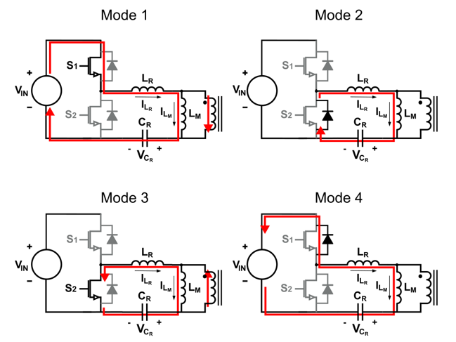
Figure 7: LLC Operating Mode Schematics
Freewheeling causes the voltage across the transistor (VDS) to drop until it reaches a value close to zero, limited by the small voltage drop of the body diode. Since this occurs when both gate signals are low, by the time the circuit transitions from Mode 2 to Mode 3 or Mode 4 to Mode 1, the voltage across the transistor is close to zero, which minimizes switching losses.
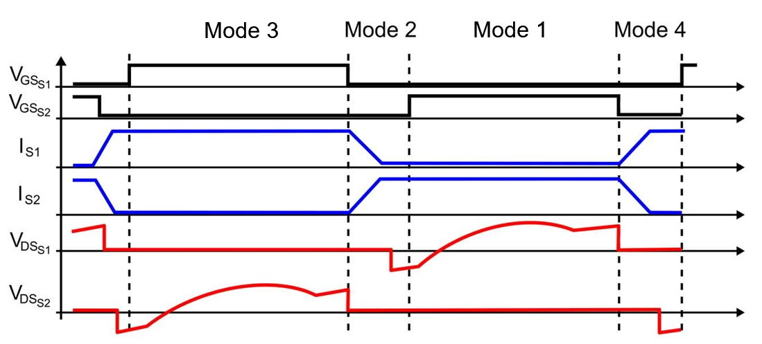
Figure 8: LLC Operating Mode Signals
Conclusion
Understanding how an LLC resonant tank operates is crucial when designing an LLC converter. The tank’s resonant characteristics make the LLC converter so popular, since this converter can maintain efficient and stable operation across a wide load and power range. However, this resonance also forces designers to be very careful when designing the circuit parameters, since the tank’s gain response depends on a multitude of parameters, including the load and the converter’s operating point (see Equation (7)).
Design tools such as the MPS LLC Designer are ideal for speeding up LLC design, allowing users to quickly iterate through different gains and frequencies and calculate the necessary component values for their design.
_______________________
Did you find this interesting? Get valuable resources straight to your inbox - sent out once per month!
Technical Forum
 Latest activity a month ago
 2 Comments
Latest activity 2 months ago
2 Comments
Latest activity 2 months ago
2 Comments
2 Comments
Latest activity 2 months ago
2 Comments
Latest activity 2 months ago
2 Comments
Log in to your account
Create New Account