Understanding Datasheet Thermal Parameters and IC Junction Temperatures

Get valuable resources straight to your inbox - sent out once per month
We value your privacy
Introduction
There is much confusion regarding how to make meaningful design decisions when converting a datasheet’s thermal resistance parameters. This introductory article will help today’s hardware engineers understand how to decipher the thermal parameters found in datasheets — including whether to choose theta vs. psi, how to calculate these values, and most importantly, how to apply these values to a design in a practical manner. This article will also describe the relationship between application ambient temperatures, and how they compare to PCB temperatures or IC junction temperatures. Lastly, it will discuss how power dissipation changes with temperature, and how to use this characteristic to achieve a cool-running, cost-optimized solution.
Electrothermal Analogy
To understand thermal quantities more easily, there are certain analogies that can be made between thermal and electrical quantities. Table 1 and Table 2 compare electrical and thermal quantities, as well as their material constants.
Table 1: Analog Relationships between Electrical and Thermal Quantities (1)
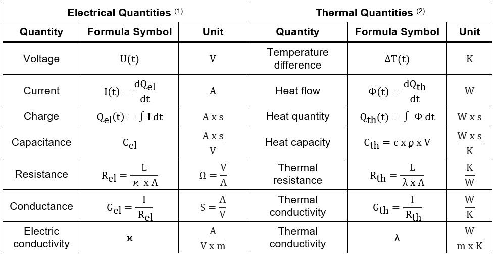
Note:
- The contents of this table are from Technische Temperaturmessung: Volume I, Frank Bernhard, ISBN 978-3-642-62344-8.
- el refers to electrical values, and th refers to thermal values.
Table 2: Material Constants and Variables for Different Materials
| Formula Symbol | Quantify | Descriptions and Examples | Values | Units |
| ρ (Greek rho) | Density | Volumetric mass density of a substance | $$kg\over {m^3}$$ | |
| λ (Greek lambda) | Thermal conductivity | Thermal conductivity of a material, ability to conduct heat | $$W\over m \times K$$ | |
| Copper | 388 | |||
| Aluminum | 205 | |||
| Silicon | 180 | |||
| Solder SAC405 (16% of Cu) | 62 | |||
| Ceramic BaTio3 (MLCCs) | 2.9 | |||
| Die attach epoxy | 2.4 | |||
| Mold compound | 1 | |||
| FR4, in-plane ↔ | 0.8 to 1 | |||
| FR4, through-plane ↕ | 0.2 to 0.4 | |||
| Air | 0.026 | |||
| κ (Greek kappa) | Electric conductivity | Material’s ability to allow the transport of an electric charge | $$1 \over \Omega \times m$$ | |
| Copper | 58.6x10⁻⁶ | |||
| Aluminum | 37.7x10⁻⁶ | |||
| Solder (13% of Cu) | 7.6x10⁻⁶ | |||
| c | Specific heat capacity | Amount of heat required to raise the temperature of 1kg of a substance by 1K | $$Ws \over kg \times K$$ | |
| Water | 4179.6 | |||
| FR4 | 1300 | |||
| Aluminum | 900 | |||
| Copper | 389 | |||
| L | Length | 1-dimensional object size | m | |
| A | Area | 2-dimensional extend of a shape | m2 | |
| V | Volume | 3-dimensional space enclosed by a boundary | m3 | |
| θJA (Greek theta) | Thermal resistance | Junction-to-air thermal resistance for a defined PCB | K/W | |
| θJC (Greek theta) | Thermal resistance | Junction-to-case thermal resistance for a defined PCB | K/W | |
| ΨJT or ΨJB (Greek psi) | Thermal resistance characteristics | Junction-to-case (top) or to-board thermal resistance. Characterized parameter based on a measurement | K/W |
Equations for Electrical and Thermal Analogy
Electrical and thermal quantities can be calculated in networks, and are comparable to Kirchhoff’s rules (see Table 3).
Table 3: Analogy between the Equations of Electrical and Thermal Processes (3)
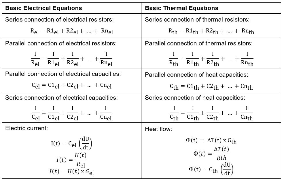
Note:
3. The contents of this table are from Technische Temperaturmessung: Volume I, Frank Bernhard, ISBN 978-3-642-62344-8.
Thermal Resistance (θJA and θJC) in a Datasheet
Figure 1 introduces the MPQ4572, a DC switching power IC from MPS, as an example for understanding thermal parameters. In this datasheet, there are two specified thermal resistance parameters: θJA and θJC. These parameters will be discussed in greater detail within this article.
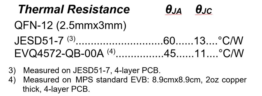
Figure 1: Thermal Resistance (θJA and θJC) Specifications in a Datasheet
Figure 2 shows a typical MPQ4572 application circuit with a 5V/2A output.
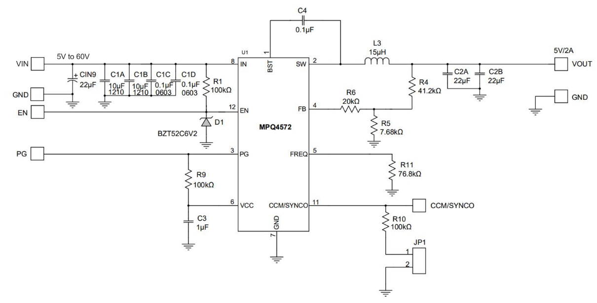
Figure 2: MPQ4572 Typical Application Circuit with a 5V/2A Output
What is the Junction-to-Ambient Thermal Resistance (θJA)?
θJA is defined as the thermal resistance from the junction to ambient temperature. It is a measure of the device’s ability to dissipate heat from the junction to ambient temperature via all heat transfer paths, the sum of copper tracks, vias, and air convention conditions.
Therefore, a given θJA is only valid for its defined PCB. It is a common mistake to believe that θJA is a constant that can be used on all PCBs. θJA allows for comparison of different packages on a common PCB, such as a JEDSD51-7. For example, if the MPQ4572 is on a 4-layer JESD51-7 PCB (4), its θJA can be calculated with Equation (1):
$$\theta_{JA} = 60 \frac{K}{W}$$Note:
4. JESD51-7 is a 4-layer PCB, and is a highly effective thermal conductivity test board for leaded surface-mount packages. It is 114.3mmx76.2mm. Its measurement method is available on https://www.jedec.org/.
If the MPQ4572 is on a 4-layer, 2oz. copper MPS test PCB (8.9cmx8.9cm), its θJA can be calculated with Equation (2):
$$\theta_{JA} = 45 \frac{K}{W}$$Figure 3 shows the EVQ4572-QB-00A, an evaluation board for the MPQ4572.
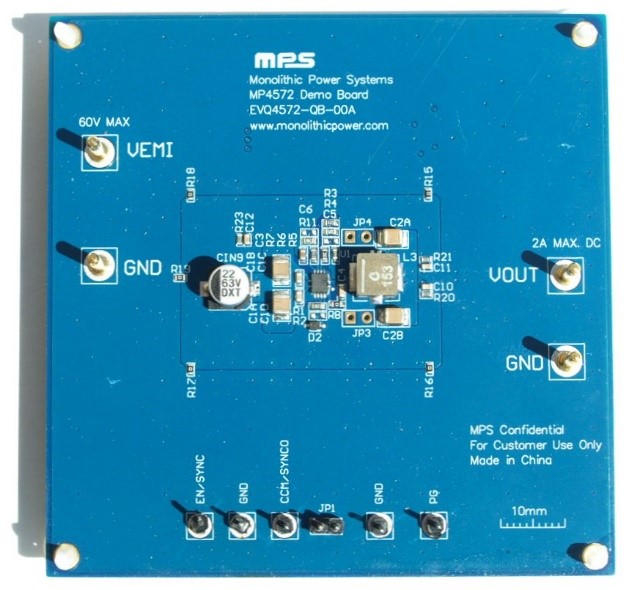
Figure 3: The EVQ4572-QB-00A Evaluation Board
The EVQ4572-QB-00A has a 1.1W dissipation when RT = 25°C. With the JESD51-7 board, the junction temperature (TJ) can be estimated with Equation (3):
$$T_J = 60 \times \frac{K}{W} \times 1.1W + 25º = 91ºC $$What is the Junction-to-Case Thermal Resistance (θJC)?
θJC is defined as the thermal resistance from the junction-to-case temperature on the bottom of the package. This temperature is measured close to the pins. Calculate the junction temperature with θJC and Equation (4):
$$T_J = (θ_{JC} \times Heatflow_{JC}) + T_C$$Where HeatflowJC is the heat flowing from the junction to case. HeatflowJC can be estimated with Equation (5):
$$Heatflow_{JC} = Heatflow_{TOTAL} -Heatflow_{JT}$$Where HeatflowJT is the heat flowing from the junction to the top surface. Figure 4 shows why θJC cannot be used as a measurement on a custom PCB.
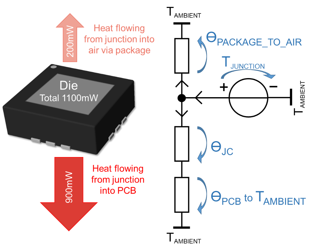
Figure 4: Junction-to-Case Thermal Resistance (θJC)
θJC cannot be used for a measurement on a custom PCB for two reasons:
- A custom PCB can be any dimension, which may be different from a JESD51-7 PCB with its fixed 114.3mmx76.2mm dimensions. The purpose of θJC is to compare the ability to transmit heat of different packages, so a JEDSD51-7 PCB should be used for that comparison since its parameters have already been studied and measured.
- The actual heat flowing from a custom PCB package is unknown, whereas a JEDSD51-7 PCB has already had this parameter measured. Consider the example with 1.1W dissipation. In the example, heat flow is separated in two paths: θJC (unknown for the custom PCB), and the heat flow that radiates via convection from the surface of the package to the environment.
What Are the Thermal Characterization Parameters for the Junction-to-Case Top (ΨJT) and Junction-to-Board (ΨJB)?
The name of the Greek letter Ψ is psi. ΨJT and ΨJB are described in JESD51-2A. Psi can be used when the designer knows the total electrical device power. Device power is often easy to measure, and by calculating it with psi, the user can directly calculate a board’s junction temperature.
ΨJT and ΨJB are virtual parameters characterized by a measurement under a specified environment. The junction temperature can be calculated with Equation (6):
$$T_J = \Psi_{JT} \times P_{DEVICE} + T_{SURFACE} $$Where TSURFACE (°C) is the temperature on top of the package, and PDEVICE is the electrical power in the IC.
Equation (6) uses the device’s total power dissipation. This means that it is not necessary to know the power distribution between the package top and pins. This is an advantage of using thermal characterization parameters instead of θJC.
A typical value for ΨJT is between 0.8°C/W and 2.0°C/W. Smaller packages tend to have a lower ΨJT, whereas larger packages with a thicker mold compound have a greater ΨJT. Estimate the difference between theta (θ) and psi (Ψ) with Equation (7) and Equation (8), respectively:
$$\theta_{12} = \frac {T_{position1} - T_{position2}} {Power_{Path12}}$$ $$\Psi_{12} = \frac {T_{position1} - T_{position2}} {P_{Device}}$$Calculation with Thermal Networks
Figure 5 shows a thermal network that can be converted into an equivalent linear electrical network. θJA is the typical name for the equivalent thermal resistance between the junction and ambient air.
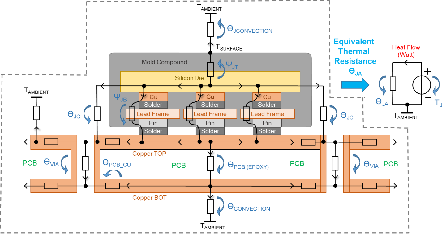
Figure 5: Drawing of a Thermal Network of an IC and a PCB
The use of thermal resistance (°C/W), heat flow (in W), and temperature difference (in Kelvin) describes the system when it has thermal stability. If you add the heat capacities (Ws/K) to this network, a transient response can be calculated.
As the size of the network and the level of detail increases, such calculations become more and more complex. The hardware developer often lacks precise information about dimensions, material constants, and heatflow. Layout and thermal programs, which can graphically represent the heat distribution via a finite element calculation, are a good choice to avoid larger mathematical calculations.
Layout Recommendations
To keep the device cool, it is recommended to make the metallic heat transfer path between the IC and copper plane as short as possible. Use two points with a large temperature difference to assist the metallic heat transfer path between cold and hot temperatures. In this system, VIA1 has a higher copper temperature difference between the top and bottom layers, compared to the colder VIA2 (see Figure 6). This means that VIA1 can transport a greater heat flow between both layers, which results in more effective cooling. Vias placed close to the package are most effective.

Figure 6: Thermal Image of DC Switching Power IC
It is essential to place a continuous copper heat path near the IC. Avoid cutting planes with unnecessary conductor tracks. Outer layers are best able to radiate heat to the environment. Avoid providing thermal relief for parts that are placed close to the IC, as the relief impairs heat transportation.
Vias improve the heat flow between layers. GND and stable potentials are suitable places for thermal vias. Filled and capped vias improve thermal conductivity, and can be placed directly under surface-mount technology (SMT) pads. A massive thermal layout is often advantageous for electromagnetic compatibility (EMC). Avoid vias with high dI/dt or du/dt (e.g. the switching node), as this worsens EMC performance.
FR4, a widely used PCB epoxy material, has low thermal conductivity, as its epoxy resin and glass fiber cannot conduct heat well. Place copper vias between the PCB layers to improve the thermal connection between layers. Certain PCB materials are 4 to 8 times more thermally conductive than FR4.
Conclusion
The MPQ4572 from MPS was used to show how thermal parameters are analogous to electrical quantities and networks, and that both can be converted into one another. The electrical quantities often used by engineers enable a quick understanding of the thermal parameters in the interactions between a PCB, environment, and semiconductor.
Thermal resistance parameters (θJA and θJC), which are commonly listed in a device’s datasheet, allow designers to compare between the thermal characteristics of different packages. Characterized thermal resistance (ΨJT and ΨJB) allows designers to calculate the junction temperature for custom applications. A temperature measurement on the top of the IC’s surface makes it simple to obtain an accurate junction temperature.
_______________________
Did you find this interesting? Get valuable resources straight to your inbox - sent out once per month!
Technical Forum
 Latest activity 3 years ago
 2 Comments
Latest activity 3 years ago
2 Comments
Latest activity 2 years ago
6 Comments
2 Comments
Latest activity 3 years ago
2 Comments
Latest activity 2 years ago
6 Comments
Log in to your account
Create New Account