Scalable Automotive Power Supply for AMD Xilinx ZU+
DOWNLOAD THE FULL REFERENCE DESIGN

Get valuable resources straight to your inbox - sent out once per month
We value your privacy
Description
This reference design is a power supply for automotive applications using the AMD Xilinx Zynq Ultrascale+ family of SoC (System on Chip) from the ZU2CG to the ZU5EG, using a flexible configuration based on multiple small DC/DC converters as PoL (Point of Load) supplies.
The MPQ8886, with its dual 3A output and multi-IC operation, allows scalability to meet the specific needs of each ZU+ device and achieve the most cost-effective solution. The MPQ8886’s outputs can be paralleled with a single inductor to reduce cost, or used in 180º phase interleave to improve transient response and reduce the input capacitance and filtering needed to pass automotive EMC qualification. The number of individual MPQ8886 IC needed will depend on the ZU+ device power needs on the VCCINT rail.
Furthermore, the MPQ8886’s digital interface allows output adjustment to optimize power consumption, as the output voltage can be modified on the go, and individual phases can be powered down if the power draw is low.
Features
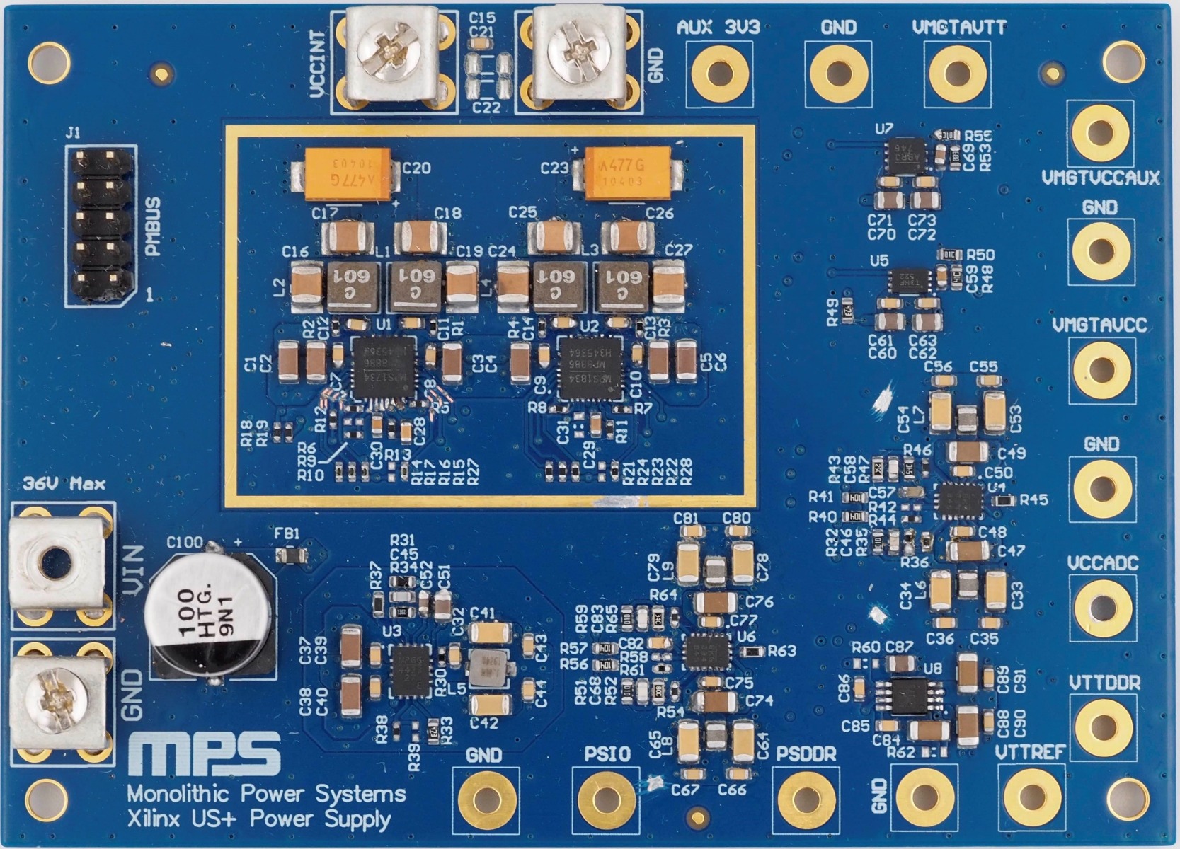
Figure 1: Evaluation Board
- AEC-Q100 Qualified
- CISPR-25 Class 5 Compliant
- Wide 5V to 35V operating input range
- -40ºC to +125ºC operating temperature range
- Scalability to meet ZU+ power needs
- AAM mode to reduce power in light-load condition
- Configurable frequency range: 150kHz to 2MHz
- OVP, UVP, OCP, UVLO and Thermal protections
- Programable Frequency Spread Spectrum for low EMI
- Multiple Times Programable memory to define default power-on conditions, with CRC protection
Applications
- Automotive Cockpit
- Automotive Infotainment
- V2X Communication
- Motion control
Application Block Diagram
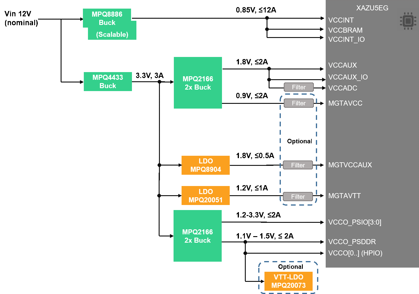
Block Diagram
Related Solutions
| MPS Integrated Circuit | Description |
| MPQ8886-0000-AEC1 | 4V-45V Input, Dual 3A / Single 6A Outputs, Digital Programmable Synchronous Buck Converter, AEC-Q100 Qualified |
| MPQ4433-AEC1 | 3.3V-36V Input, 3A Synchronous Buck Converter. AECQ-100 Qualified |
| MPQ2166A-AEC1 | 2.7V-6V Input, Dual 2A/2A or 3A/1A Outputs, Synchronous Buck Converter, AEC-Q100 Qualified |
| MPQ8904-AEC1 | 2.5V-6.5V Input, 500mA Linear Regulator, AEC-Q100 Qualified |
| MPQ20051-AEC1 | 2.5V-5.5V Input, High PSRR 1A Linear Regulator, AEC-Q100 Qualified |
| MPQ20073-AEC1 | 1.3V-6V VDDQ, 2A DDR Memory Termination Regulator, AEC-Q100 Qualified |
Table 1: MPS Solutuions
System Specifications
| Parameter | Specification |
| Input Voltage Range | 4VDC to 36VDC |
| Output Voltage | Multiple Outputs |
| Maximum output current | 12A on VCCINT |
| Switching frequency | 600kHz, 1MHz |
| Board form factor | 99mmx70mmx5mm |
| Power-on sequencing | Yes |
| Power-off sequencing | No (Needs external sequencer) |
Table 2: System Specifications
| Power Rail | Electrical Characteristics | Source | Power-on Sequence |
| VCCINT / VCCBRAM / VCCINT_IO | 0.85V ±3%, ≤12A | 2x MPQ8886 | 1 |
| VCCAUX / VCCAUX_IO / VCCADC | 1.8V ±2%, ≤2A | MPQ2166A | 2 |
| VMGTAVCC | 0.9V ±2%, ≤2A | MPQ2166A | 2 |
| VMGTVCCAUX | 1.8V ±2%, ≤0.5A | MPQ8904 | 3 |
| VMGTAVTT | 1.2V ±2%, ≤1A | MPQ20051 | 3 |
| VCCO_PSDDR | 1.1V-1.5V ±3%, ≤2A | MPQ2166A | 3 |
| VCCO_PSIO [3:0] | 1.8V-3.3V ±3%, ≤2A | MPQ2166A | 3 |
| VTT | 0.5·VCCO_PSDDR, 2A | MPQ20073 | 4 |
Table 3: ZU+ Rails Distribution
Test Results
Efficiency
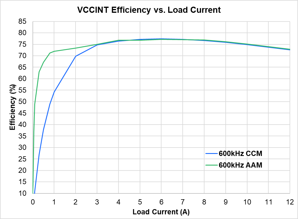
Figure 15: VCCINT Efficiency - VIN = 12V, TA = 25 - VOUT = 0.85V, FSW = 600kHz, L = 600nH, 4 phases
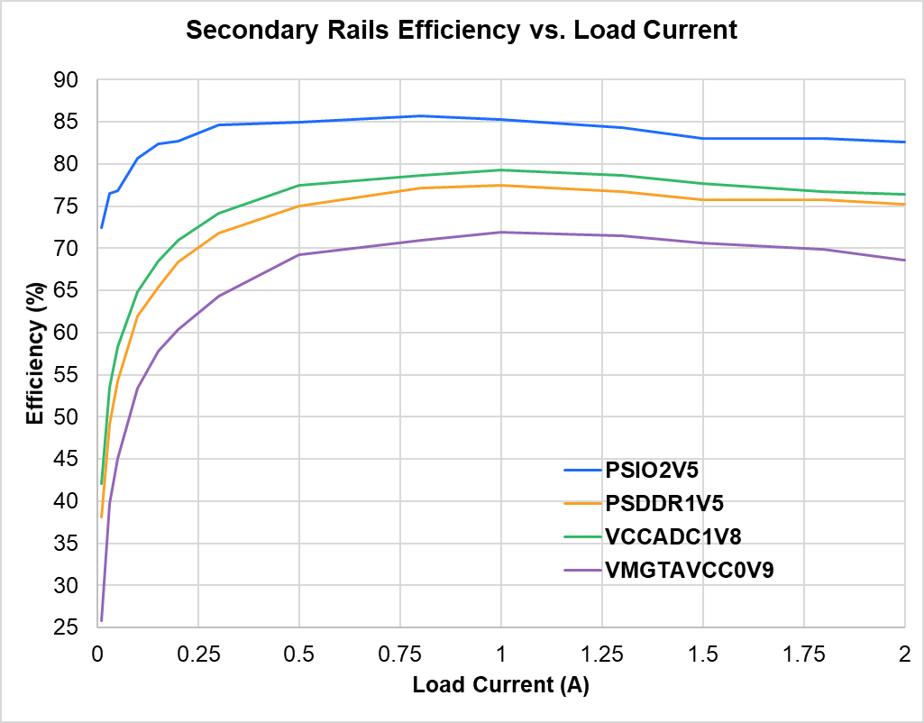
Figure 16: Secondary Rails Efficiency - MPQ4433 and MPQ2166 in series conversion
Time Domain Waveforms
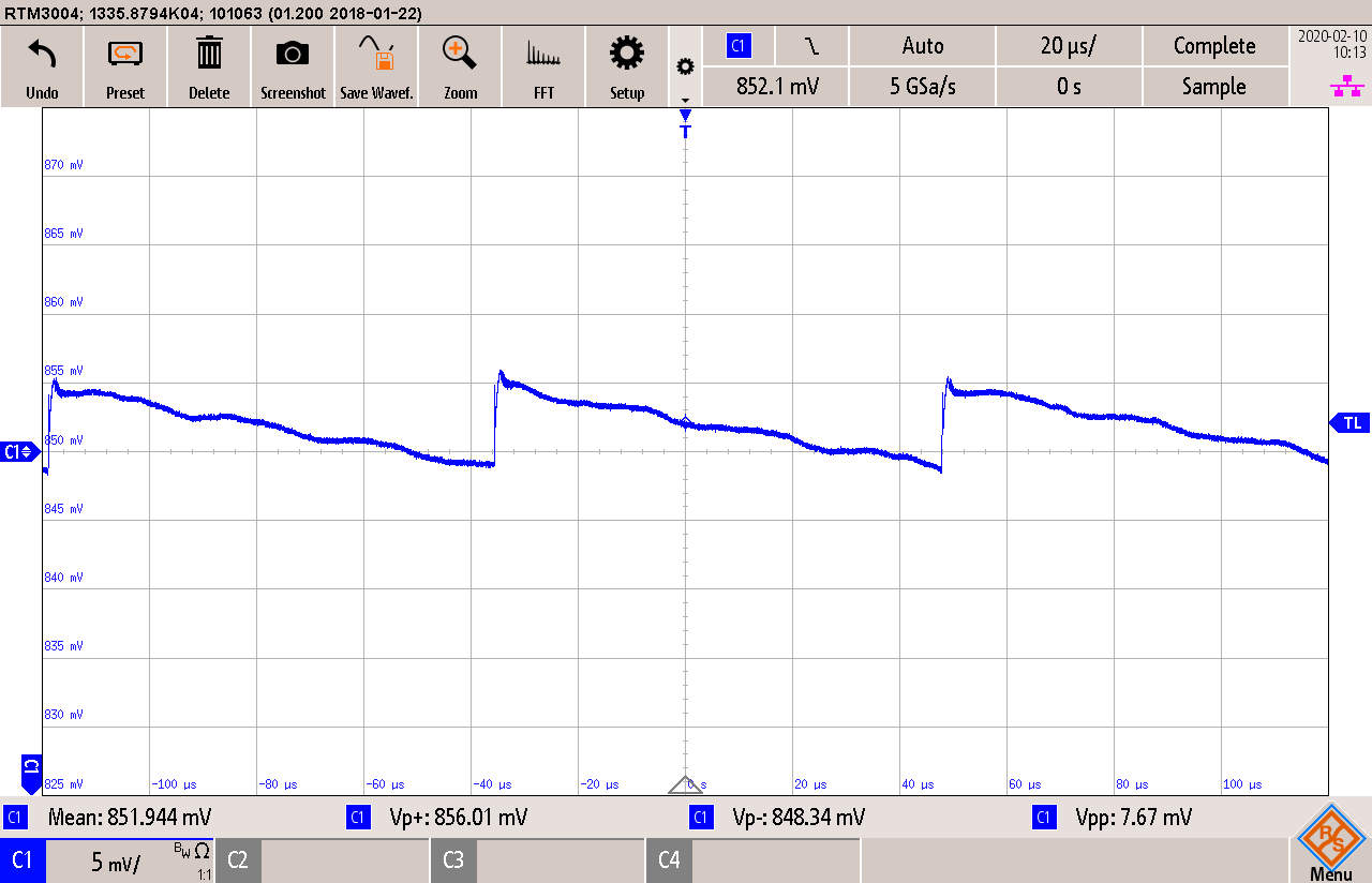
Figure 17: VCCINT Steady state - IOUT = 0A, VOUT = 0.85V - VIN = 12V, TA = 25ºC, AAM Mode
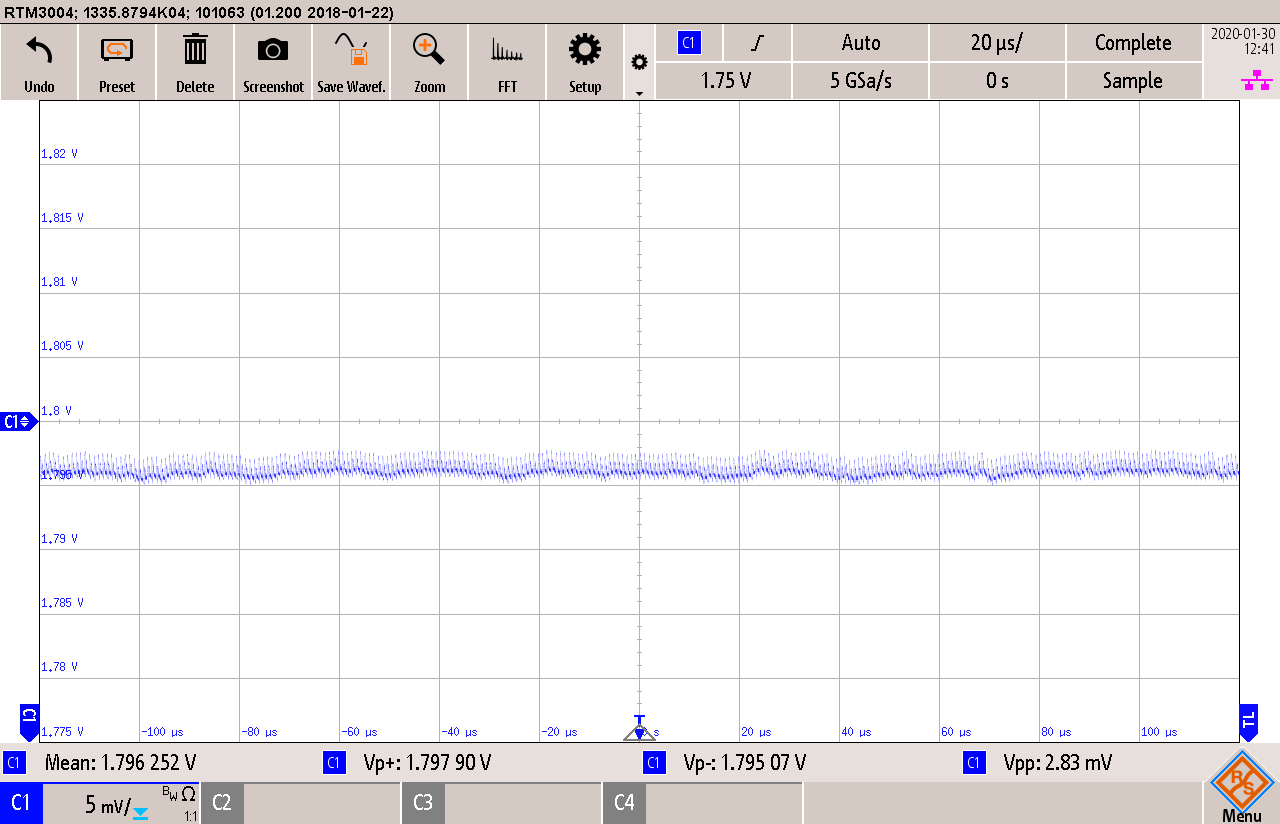
Figure 19: VCCADC Steady state- IOUT = 0A, VOUT = 1.8

Figure 21: VCCAUX Steady state - IOUT = 0A, VOUT = 1.8

Figure 23: VMGTAVCC Steady state - IOUT = 0A, VOUT = 0.9V

Figure 25: VMGTVCCAUX Steady state - IOUT = 0A, VOUT = 1.8

Figure 27: VMGTAVTT Steady state - IOUT = 0A, VOUT = 1.2

Figure 29: VCCO_PSDDR Steady state - IOUT = 0A, VOUT = 1.5V

Figure 31: VCCO_PSIO Steady state - IOUT = 0A, VOUT = 2.5V
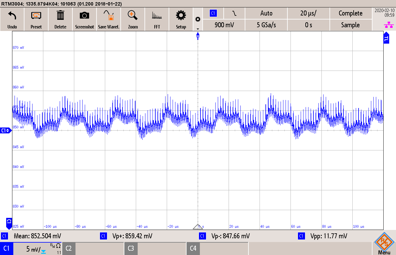
Figure 18: VCCINT Steady state - IOUT = 12A, VOUT = 0.85V
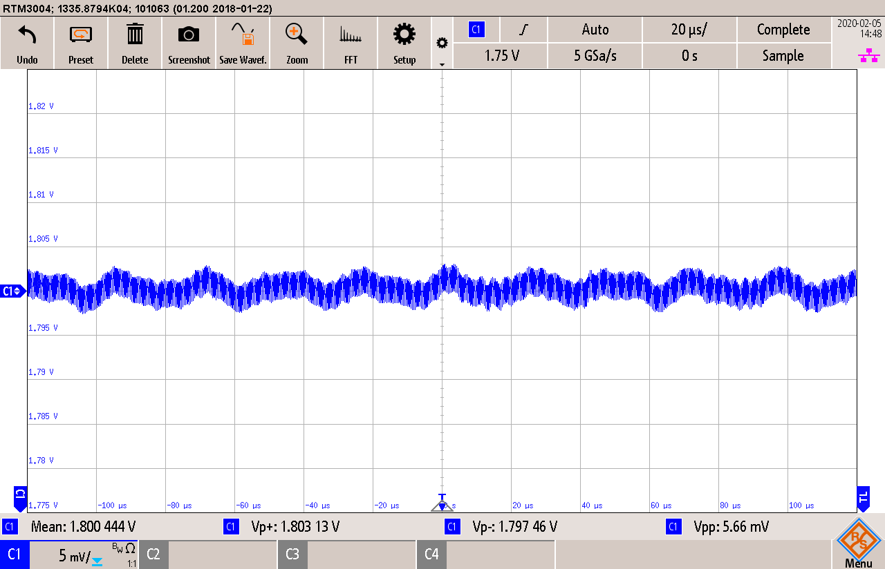
Figure 20: VCCADC Steady state - IOUT = 2A, VOUT = 1.8V

Figure 22: VCCAUX Steady state - IOUT = 2A, VOUT = 1.8V

Figure 24: VMGTAVCC Steady state - IOUT = 2A, VOUT = 0.9V

Figure 26: VMGTVCCAUX Steady state - IOUT = 0.5A, VOUT = 1.8V

Figure 28: VMGTAVTT Steady state - IOUT = 1A, VOUT = 1.2V

Figure 30: VCCO_PSDDR Steady state - IOUT = 2A, VOUT = 1.5V

Figure 32: VCCO_PSIO Steady state - IOUT = 2A, VOUT = 2.5V

Figure 33: VCCINT response to a 25% load step - IOUT = 5.5A to 8.5A, VOUT = 0.85V

Figure 34: Power-on sequence - Start from VIN
EMC Measurement
VIN = 12V; FSW_MPQ8886 = 600kHz, 10% Spread spectrum; FSW_MPQ4433 = 1MHz, TA = 25ºC
IVCCINT = 12A, IAUX_3V3 = 2A

Figure 37: CISPR25 Class 5 Conducted Emissions - 150kHz – 108MHz

Figure 38: CISPR25 Class 5 Radiated Emissions - 150kHz – 30MHz
Log in to your account
Create New Account