AN163 - Protection Functions Application Note

Get valuable resources straight to your inbox - sent out once per month
We value your privacy
The MP653x families of three-phase pre-drivers have a number of protection features to prevent damage to circuits and motors in the event of fault conditions. These features need to be set up correctly, or protection circuits may operate incorrectly. This application note discusses the various protection features of these parts, and how to properly configure them.
Applicable Parts
This application note applies to the following parts:
| Part Number | Description | Supply Voltage |
| MP6528 | H-Bridge Gate Driver | 60V |
| MPQ6528 | H-Bridge Gate Driver (AEC-Q100) | 60V |
| MP6530 | 3-Phase BLDC Motor Pre-Driver with PWM and ENBL inputs | 60V |
| MPQ6530 | 3-Phase BLDC Motor Pre-Driver PWM and ENBL inputs (AEC-Q100) | 60V |
| MP6531A | 3-Phase BLDC Motor Pre-Driver with Separate HS/LS Control | 60V |
| MPQ6531 | 3-Phase BLDC Motor Pre-Driver with Separate HS/LS Control (AEC-Q100) | 60V |
| MP6532 | 3-Phase BLDC Motor Pre-Driver with Hall Inputs | 60V |
| MPQ6532 | 3-Phase BLDC Motor Pre-Driver with Hall Inputs (AEC-Q100) | 60V |
| MP6534 | 3-Phase BLDC Motor Pre-Driver and Buck Converter | 60V |
| MP6535 | 3-Phase BLDC Motor Pre-Driver with Hall Inputs and Buck Converter | 60V |
| MP6537 | 3-Phase BLDC Motor Pre-Driver with PWM and ENBL inputs | 100V |
| MP6538 | 3-Phase BLDC Motor Pre-Driver with Hall Inputs | 100V |
| MP6539 | 3-Phase BLDC Motor Pre-Driver with Separate HS/LS Control | 100V |
INTRODUCTION
The MP653x family of gate drivers are targeted primarily at motor drive applications. They integrate power supply and control functions that help implement a motor drive. Included in their functionality are protection circuits to help prevent failures in the event of abnormal conditions, such as excessive current, short circuits, and component failures.
Many of these protection circuits require configuration using external components. If the external circuits are not correctly configured, the protection circuits may operate under conditions that are not really fault conditions. Understanding the protection mechanisms and how to set up external components is necessary to implement a properly operating motor drive. Many of the protection features are identical across all of the MP653x family of parts. Others are slightly different between the 60V drivers and the 100V drivers. In some cases, the behavior of the part is different in one part than the others. This document will cover all of the parts in this family, and will note differences between parts where applicable.
Also refer to application note AN111 for a discussion about designing with the MP653x pre-drivers.
PROTECTION FEATURES
Following is a summary of the various protection features integrated into the MP653x family of pre-drivers:
Overtemperature Protection (OTP)
Applicable parts: All
A temperature sensor integrated within the device will cause operation to stop if the temperature exceeds the overtemperature threshold listed in the datasheet. When this occurs, all outputs will be set low, disabling the motor.
Some parts latch off after OTP, and others automatically re-start. Refer to Table 1 below for details.(1)
Supply Voltage Undervoltage Lockout (VIN UVLO)
Applicable parts: All
The voltage on the main supply voltage input (VIN) is monitored by a comparator circuit. If the supply voltage is below the VIN undervoltage threshold listed in the datasheet, the device is disabled and all outputs are driven low, disabling the motor. VIN UVLO acts as a global reset to the logic in the IC. The device is enabled after the voltage rises above the threshold. Note that some time is required – typically about 1mS – after the voltage rises above the threshold before the device will drive the outputs.
Gate Drive Voltage Undervoltage Lockout (VREG UVLO)
Applicable parts: All
The output of voltage of the gate drive supply (VREG) is monitored by a comparator circuit. If the voltage is below the VREG undervoltage threshold listed in the datasheet, the device is disabled and all outputs are driven low, disabling the motor.
Some parts latch off after VREG UVLO, and others automatically re-start when VREG rises. Refer to Table 1 below for details.
High-Side Gate Drive Voltage Fault (VBST UVLO)
Applicable parts: MP6537, MP6538, MP6539
A circuit monitors the voltage present on each of the BSTx pins, which is the gate drive voltage for each high-side MOSFET. The capacitor connected to the BSTx pin is charged to VREG every time the output (SHx) is driven low. It is also charged by a very weak current supplied from an internal charge pump, which allows the output to be held high for an extended period of time.
When a VBST UVLO occurs, the high side gate will be turned off until the next time it is commanded to turn on. VBST UVLO does not cause nFAULT to be asserted,
Short Circuit Protection (SCP, or VDS Sensing)
Applicable parts: All
A circuit monitors the voltage drop across a MOSFET that is turned on. If the MOSFET is not fully turned on, as evidenced by a low voltage drop across it, SCP protection is activated.
Generally, the threshold for when the SCP fault is detected is set by the voltage applied to the OCREF pin. The 100V parts do not use the OCREF voltage to sense the high-side MOSFET – they will signal a VDS fault if, when the output is driven high, it does not exceed a fixed threshold of about 4.5V.
Some parts latch off after SCP, and others automatically re-start. Refer to Table 1 below for details.
Overcurrent Protection (OCP, or Motor Current Sensing)
Applicable parts: All
A single shared low-side shunt resistor may be used to measure the total motor current. This shunt resistor is connected to the LSS pin. If the voltage drop across the shunt exceeds some threshold, an OCP event is recognized.
60V parts have a fixed threshold of 500mV at the LSS pin. 100V parts have a fixed threshold of 3.5V at the CSO pin; the CSO pin is driven by an amplifier with a gain of 20 from the LSS pin, so the equivalent voltage at LSS is 175mV.
Some parts latch off after OCP, and others automatically re-start. Refer to Table 1 below for details.
| Feature | MP6528, MP6530, MP6534, MP6535 | MP6532 | MPQ6532 | MPQ6528, MPQ6530 | MP6531A, MPQ6531 | MP6537, MP6538, MP6539 |
| OTP | Latch off (1) | Latch Off (1) | Retry when cool | Retry when cool | Retry when cool | Retry when cool |
| SCP | Latch off (1) | Latch Off (1) | Latch Off (1) | Latch Off (1) | Latch Off (1) | High side: Latch off (1) Low side: Retry after adjustable time |
| OCP | Latch off (1) | Retry after fixed time | Retry after fixed time | Latch Off (1) | Latch Off (1) | Retry after adjustable time |
| VREG UVLO | Latch off (1) | Latch Off (1) | Latch Off (1) | Retry when > UVLO | Retry and initiate BST charge | Retry and initiate BST charge |
Table 1: Protection Behaviors
(1) Latch off is reset by removal / re-application of VIN, or assertion / de-assertion of nSLEEP
MOSFET SWITCHING BEHAVIOR
An understanding of the switching behavior of the MOSFETs being driven by the MP653x pre-driver is needed to prevent inadvertently triggering the protection circuits. In particular, the VDS sensing can be easily triggered under some conditions.
MOSFET Gate Capacitance
When the high side MOSFET is turned on, the gate is driven primarily by the charge that is stored in the bootstrap capacitor. If the gate capacitance is very high, and if there is not enough charge stored in the bootstrap capacitor, the high side MOSFET may not be fully turned on. This can result in a VDS fault from the high side. Often, using a larger capacitor on the BST pin can improve this situation.
In addition, at high PWM frequency, the amount of current needed to drive the gates increases. In some cases, it is possible to cause a VREG UVLO fault. When using large MOSFETs and high PWM frequencies, it is recommended to use a larger capacitor on the VREG pin to help prevent these faults.
Gate Drive Resistors
Usually, resistors are inserted between the outputs of the MP653x gate drive outputs and the MOSFET gate. These resistors limit how fast the MOSFET switches.
Dead Time
To prevent the high-side and low-side MOSFETs from conducting at the same time, which would result in a path directly from the VIN supply to ground (and very high current flow through the MOSFETs), some time must be inserted between the time one MPOSFET turns off and the other turns on. This is called dead time. The MP653x family of drivers all generate dead time during switching, regardless of the input signal timing. The dead time is programmable by the value of an external resistor connected to the DT pin.
Blanking (or Deglitch) Time
Since there is some time required for a MOSFET to switch, after a MOFET is turned on, it is necessary to wait some amount of time before checking to see if there is a problem that the OCP protection needs to operate on. This time is called blanking time. Blanking time is measured from the end of dead time until the point where the VDS sensing circuit looks at the voltage across a MOSFET.
In the 60V parts, the blanking time for SCP detection is 3μS; in the 100V parts it is 2.73μS. The MOSFET must be fully turned on by the time this time has expired, or the SCP protection will be triggered!
CONFIGURING EXTERNAL COMPONENTS
Following are some suggestions about the configuration of the external components that may affect the protection features of the MP653x predrivers.
MOSFET Gate Resistors
Typically, the resistors (or resistor/diode network) between the MP653x and the MOSFET gate are determined by the required rise/fall times at the output. Faster is preferred to minimize switching losses; slower is preferred to generate less EMI.
In any case, it is imperative that the rise/fall time is less than the blanking time, as described above. If the MOSFET has not fully turned on by the expiration of the blanking time, SCP will be triggered!
The gate of a power MOSFET can be viewed as a nonlinear capacitance between the gate and source terminals. Even though the gate does not conduct DC current, current is needed to charge and discharge the gate capacitance to turn the MOSFET on and off. The amount of current provided to the gate determines how much time it takes to fully turn on the MOSFET. Similarly, when current is pulled out of the gate, that amount of current sets the MOSFET turn-off time.
To understand what is needed to drive the gate, one needs to know how fast the MOSFET must be switched. There is a design tradeoff made between low switching losses (which require fast rise and fall times) and low EMI (which requires slow rise and fall times). In addition, the PWM frequency and minimum and maximum required duty cycles put a time restriction on how fast switching needs to be. For example, with a 20kHz PWM frequency, a 1% duty cycle requires generating a pulse that is 500ns long. This requires a rise and fall time of a few hundred nanoseconds or less.
After determining what rise/fall time is required, calculate the necessary gate drive current. This can be estimated as QG / t, where QG is the total gate charge and t is the desired rise/fall time.
Note that this is the amount of current that would need to be driven for the entire rise/fall time — in reality, the gate drive current usually varies somewhat over this time, as most gate drivers are not constant-current drivers.
If delivering a constant current into the gate, the voltage at the gate is not a linear slope — it reaches a plateau during the time that the MOSFET is switching (see Figure 1). This is called the “Miller plateau,” and is caused by the gate-drain capacitance. When the drain is transitioning, this capacitance takes current to charge, so the charging of the gate-source capacitance slows.
The lower the current provided to charge the gate, the longer the time that it takes the transition to complete.

Figure 1: 1A Constant-Current Gate Drive (100nC - Red = gate, purple = drain, 200ns/div.)
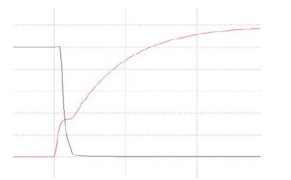
Figure 2: 12V Gate Drive with 12Ω Series Resistance(100nC - Red = gate, purple = drain, 200ns/div.)
Figure 2 shows the waveforms if a 12V constant voltage gate drive is used with 12Ω series resistance. The plateau is still there and it takes longer for the gate to reach 12V, but the switching time at the drain is nearly the same.You can get independent rise and fall times by adding a diode (see Figure 3).
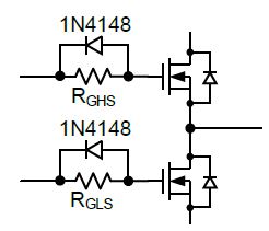
Figure 3: Diagram for Adding a Diode
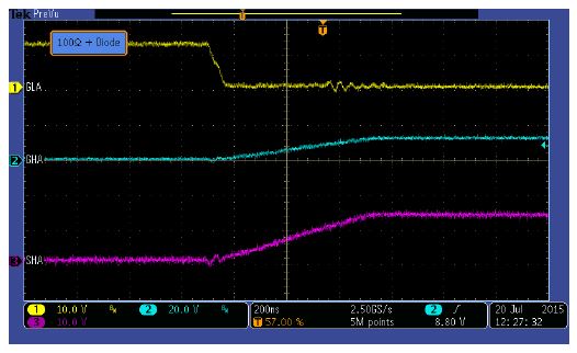
Figure 4: Gate and Output Waveforms
This is often done to ensure that one FET in a half-bridge arrangement turns off fully before the opposing FET turns on, which guarantees dead time. Figure 4 shows that the low-side gate (GLA) drops very quickly as it is discharged through the diode, but the high-side gate (GHA) charges slowly due to the resistor. The result is a slow rise time at the output (SHA), controlled by the high-side MOSFET turn-on.
Since the gate has a nonlinear capacitance and the driver is usually not a true voltage or current source (typically it is a FET operating in a linear region), it can be difficult to accurately calculate the necessary resistance to achieve a specific rise or fall time. It is usually best to derive the right values experimentally, or through simulation. Start with the assumption that the gate drive current will equal the gate drive voltage (often 12V) divided by the series resistance, and work from there. Be sure to also include the output resistance of the gate driver when making this calculation.
The MP653x pre-drivers have internal pull down resistors on the gate drive outputs. Placing external resistors from drain to source of the MOSFETs is not required. Putting gate to source resistors on the high side MOSFETs can cause OCP faults, by discharging the BST capacitors. This is discussed further below.
Dead Time Resistor
MP653x pre-drivers have a programmable dead time feature. This inserts a time delay between one MOSFET in a half bridge turning off, and the other turning on.
Dead time in the MP653x devices is programmed with a single resistor to ground. Dead time can be programmed over a wide range, from 30nS to 6μS for 60V parts and 77nS to 4.6μS for 100V parts.
The resistor value is calculated as follows:
$$60V parts: t_{DEAD}(nS) = 3.7*R(kΩ)$$ $$100V parts: t_{DEAD}(μs) = 0.044*R(kΩ) + 0.1$$Note that the blanking time for SCP does not begin until the end of dead time.
Bootstrap (BST) Capacitors
Bootstrap capacitors provide the large peak currents needed to turn on the HS MOSFET. These capacitors are charged when the output is driven low, and then the charge in the bootstrap capacitor is used to turn on the HS MOSFET when the output is driven high. Note that an internal charge pump keeps the bootstrap capacitor changed when the output is held high for an extended period.
Bootstrap capacitors need to be large enough so that the high side MOSFET is turned fully on. If not, then the VDS across the high side MOSFET will increase, and may trigger the SCP.
Bootstrap capacitors are selected depending on the MOSFET total gate charge. When the HS MOSFET is turned on, the charge stored in the bootstrap capacitor is transferred to the HS MOSFET gate. As a simplified approximation, the minimum bootstrap capacitance can be estimated as follows:
$$C_{BOOT} > 8*QG$$Where QG is the total gate charge of the MOSFET in nC, and CBOOT is in nF.
Bootstrap capacitors should not exceed 1μF, or they may cause improper operation at start-up. For most applications, bootstrap capacitors should be between 0.1μF and 1μF, X5R or X7R ceramic, rated for 25V minimum.
VREG Bypass Capacitor
The high peak currents needed to charge the low side MOSFET gate and also the bootstrap capacitor comes primarily from the VREG bypass capacitor. The VREG supply can only drive a limited DC current. Using too small of a capacitor can result in low gate drive voltages, which can trigger SCP protection.
It is recommended to use a minimum 10μF, X5R or X7R ceramic capacitor, rated for 25V minimum. Larger capacitors can be used with very large MOSFETs and/or very high PWM frequencies.
Overcurrent Protection (LSS Sense Resistor)
Overcurrent protection senses the motor current using a single shared low-side shunt resistor that is connected to the LSS pin. The voltage drop across that resistor, if it exceeds the OCP threshold (as described above), will trigger OCP.
Note that the behavior during OCP varies from part to part. Refer to Table 1 above for details. The external sense resistor is sized to provide a drop less than 500mV (60V parts) or 175mV (100V parts) at the maximum expected motor current. For example, if a 50mΩ resistor is used, a current of 10A will cause a 500mV drop, and activate the over-current protection of a 60V part.
Margin needs to be added so that the OCP protection does not trigger during higher than normal motor current. The stall current at motor start-up must be considered, as well as current pulses that result from commutation. Note that some mis-commutation often occurs, sometimes more in one rotation direction than the other, that results in current spikes at each commutation point.
If this function is not needed, connect LSS to ground directly.
OCREF voltage (SCP Threshold)
SCP detection level is programmed by the voltage applied to the OCREF pin. This voltage sets the threshold at which OCP is triggered. If the VDS of a MOSFET, after the blanking time, is higher than OPCREF, OCP is triggered.
At a minimum, OCREF voltage must be higher than the expected voltage drop across all MOSFETs at the highest expected load current. The rds(on) of MOSFETs varies considerably, especially at high temperature. In addition, at high currents, the PCB trace resistance may approach that of the MOSFET. Because of this, typically OCREF must be set considerably higher than an initial calculation might predict. Typically, setting OPCREF to 2x the calculated maximum is required.
Again, peak currents during times like commutation must also be considered, to prevent undesired OCP protection activation.
CSO Pin Resistor and Capacitor (100V parts only)
Whenever the CSO pin exceeds 3.5V, an OCP event is detected, and all output FETs are turned off. The nFAULT pin will be driven active low.
Once current through the low-side FETs and the sense resistor stops, the voltage on the CSO pin is no longer driven, and it starts to fall at a rate determined by the external capacitor and resistor connected from CSO to ground. When the voltage falls below 2.9V, the output FETs are re-enabled, and the nFAULT pin is made inactive.
The resulting off time is set by the value of the external capacitor and the internal feedback resistor in parallel with the external resistor (if used). The off time generated when CSO reaches 3.5V can be approximated by to the following formula
$$t_{OFF} (μS) = 0.2*R(kΩ)*C(nF)$$The off time generated after a SCP (when VDS exceeds OCREF) is longer, since CSO gets pulled to 6V and must decay to 2.9V for the outputs to be re-enabled. This off time can be approximated by to the following formula
$$t_{OFF} (μS) = 0.6*R(kΩ)*C(nF)$$Where C is the capacitance from CSO to ground, and R is the total resistance from CSO to ground, comprised of the internal feedback resistor (~450kΩ) in parallel with any external resistor to ground.
BOOTSTRAP PRE-CHARGE
Although not a protection feature, attention should be paid to pre-charging the bootstrap (BST) capacitors in some cases. Enabling a high side MOSFET when there is insufficient charge in the BST cap may result in an SCP fault, due to the inadequate charge not fully enhancing the high side MOSFET. Pre-charging the BST capacitors is accomplished by turning on the low side MOSFET for a short period of time.
This can be problematic particularly during 120-degree commutation, where a phase is left in the high impedance state for some time. If there is leakage current, the BST capacitor may become discharged during this time. It is also very important to not place any gate-to-source resistors on the high side MOSFETs, as this would cause the BST capacitors to be discharged.
Some MP653x parts perform an automatic bootstrap charge sequence under certain conditions. The automatic sequence consists of turning on each low side MOSFET sequentially for a very short period (1.8μS for 60V parts, 4.6 μS for 100V parts). Automatic bootstrap charge is done according to Table 2 below.
| MP6528, MP6530, MP6532, MP6534, MP6535 | MP6531A, MPQ6531, MP6537, MP6538, MP6539 |
| Automatic pre-change when exiting from high-Z state (1) | Automatic pre-charge after recovery from VREG UVLO (2) |
Table 2: Bootstrap Pre-Charge
(1) During 120-degree commutation, these parts will automatically perform a boost pre-charge when exiting the high impedance commutation phase
(2) During 120-degree commutation, it is recommended that the controller perform a boot cap charge, or drive the phase low before driving it high, when exiting the high impedance commutation phase
Although the internal charge pump will charge the bootstrap capacitors, it takes some time after VREG UVLO for the capacitors to be charged, as the internal charge pump can only drive a very small current. If a high side MOSFET is turned on before the BST cap has been charged, an OCP fault may be triggered due to insufficient charge in the BST cap. This can be prevented by driving the output low (low side MOSFET on) before turning on the high side FET. Passive pull down resistors on the outputs (SHx pins) will also help ensure that the BST capacitors are charged.
DISABLING PROTECTION FEATURES
If the system does not require the MP653x SCP and OCP protection features, they can be disabled by connecting the OCREF pin through a 100k resistor to VREG. The VIN UVLO and VREG UVLO functions will continue to operate.
Log in to your account
Create New Account