Optimizing Power Supply Efficiency with MOSFET Selection

Get valuable resources straight to your inbox - sent out once per month
We value your privacy
Introduction
When designing power supplies, it is always critical to optimize the design for efficiency. Increased efficiency saves energy, reduces heat generation, and can even reduce the power supply’s size.
This article will discuss how to choose the ratio between the number of high-side MOSFETs (HS-FETs) and low-side MOSFETs (LS-FETs) to improve efficiency in power supply designs.
Figure 1 shows a simplified circuit with an HS-FET and LS-FET
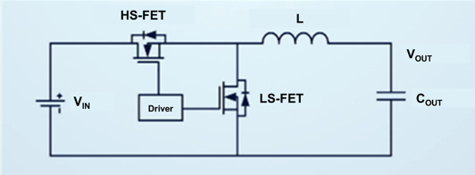
Figure 1: Circuit with an HS-FET and LS-FET
When selecting MOSFETs, power engineers may struggle to distribute the internal resistance of the HS-FET and LS-FET for optimal efficiency.
MOSFET Structure and Loss Composition
When selecting a MOSFET with efficiency in mind, the designer must optimize between conduction loss and switching loss. Conduction loss occurs when the MOSFET is closed, and is due to current flowing through the on resistance. Switching loss occurs when turning the MOSFET on and off, and is due to the fact that the MOSFET does not switch on and off immediately. This is caused by the capacitive behavior of the semiconductor structure within the MOSFET.
A MOSFET is an integrated, multi-component structure that is comprised of multiple MOSFET semiconductor structures connected in parallel. There is a tradeoff between resistance and capacitance. The more MOSFET crystals are connected in parallel, the smaller the on resistance (RDS(ON)), but the larger the parasitic capacitance. A small RDS(ON) reduces conduction losses but increases parasitic capacitance, which then increases switching losses.
Selecting MOSFETs requires significant consideration, and onboard testing can require too much time and resources. Therefore, it is more advantageous to create an accurate mathematical model to analyze losses and help with MOSFET selection.
Related Content
-
ARTICLE
Understanding AC/DC Power Supplies
Discover how to choose the ratio between the number of high-side MOSFETs (HS-FETs) and low-side MOSFETs (LS-FETs) to improve efficiency in power supply designs.
-
WEBINAR
Driving Power MOSFETs Webinar On Demand
Learn more on how to drive the gates of power MOSFETs
-
ARTICLE
MOSFET Switches: Basics and Applications in Power Converters
MOSFETs are an integral part of nearly all electronic systems, read to learn more
-
VIDEOS

Design a 600W LLC Converter for a PC Power Supply
Learn how to design an LLC converter, including the inductor and transformer
Calculating Conduction Loss
First, calculate conduction loss, as this is a relatively simple calculation. In a single cycle, the conduction loss can be calculated by considering the current flowing through the MOSFET and the ripple current.
For accuracy, consider the relationship between RDS(ON) and temperature when making this calculation. The MOSFET’s internal resistance is not a fixed value, and it increases as the temperature increases.
Figure 2 shows how to calculate conduction loss, where IO is the nominal current, ΔIO is the current ripple amplitude, TJ is the junction temperature, and k is the temperature coefficient.
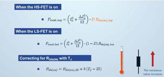
Figure 2: Conduction Loss Calculation
Switching Loss (Parasitics)
It can be difficult to calculate switching loss. When making this calculation, consider the parasitic inductance caused by the inductors in each loop, as well as the MOSFET’s nonlinear parasitic capacitance at different voltages.
Figure 3 shows the two types of parasitic components to consider when calculating the switching loss.
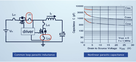
Figure 3: Two Types of Parasitic Components
Switching Loss (Turn-On Loss)
There are three stages for turn-on loss, described below.
- Stage 1 (HS-FET stage): When the HS-FET turns on, the drain-to-source voltage (VDS) begins to drop. In contrast, the drain-to-source current rises until the HS-FET’s VDS(TOP) voltage drops to 0V, or the HS-FET current (IHS) rises to the output current (IOUT).
- Stage 2 (reverse recovery stage): During reverse recovery, ITOP reaches its peak value, and the LS-FET starts to build up its voltage.
- Stage 3 (oscillation stage): Oscillation ends when IHS stops fluctuating.
Figure 4 shows the switching losses related to turn-on loss.
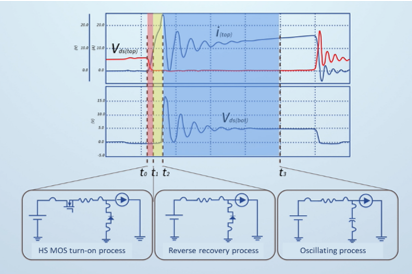
Figure 4: Turn-On Loss
Switching Loss (Turn-Off Loss)
There are two stages for turn-off loss, described below.
Stage 1 (DS voltage rising): As VDS rises, IDS falls. This stage ends when IDS drops to 0A.
Stage 2 (oscillation): Oscillation continues until VDS stops oscillating.
Figure 5 shows the turn-off loss.
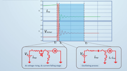
Figure 5: Turn-Off Loss
Mathematical Model and Analytical Validation
After understanding the circuit’s various losses, it is time to establish a mathematical model.
- Set the required circuit parameter values. The MOSFET values should be analyzed using the equations above, as well as their nonlinear parameter compensation values.
- Run a transient simulation over at least one switching period for the converter while in steady state operation.
- Integrate the voltage and current waveforms to obtain the MOSFET’s switching loss and conduction loss. This can be accomplished using a power probe or by multiplying the current and VDS waveforms.
Once the model is available, use the data obtained from the power losses found above to obtain the simulated efficiency, and compare that value to the efficiency curve obtained from the board (or the datasheet). If the calculation’s efficiency error is within 0.5%, the model is accurate (see Figure 6).
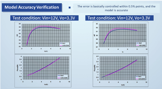
Figure 6: Mathematical Model Verification
MOS Selection Based on Mathematical Tools
For this article, we used 10 MOSFETs with a total internal resistance of 100mΩ, then used the model to calculate the efficiency curves under different ratios. For example, consider a ratio of 1:9. That would mean there is one HS-FET (high RDS(ON), low capacitance) and nine LS-FETs (low RDS(ON), low capacitance).
By comparing the curves, we can conclude that the MOSFET ratio of 3:7 is the optimal specification for 12V to 3.3V, 10A applications (see Figure 7). This efficiency curve cluster shows that different ratios will result in different efficiency curves, even with the same number of MOSFETs. Find the optimal ratio to optimize your efficiency curve.
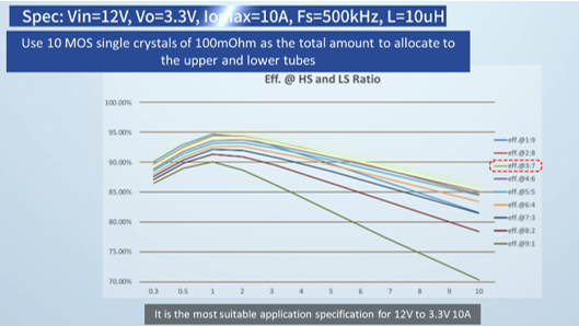
Figure 7: Optimal MOSFET Ratio
Figure 9 shows how, for the same input and output specifications, as well as the same output current, the minimum loss point in the circuit is found at different MOSFET ratios. Therefore, designers must keep these specifications in mind when selecting the MOSFET ratio.
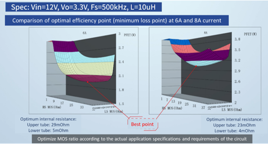
Figure 9: Optimal Efficiency Comparisons
Conclusion
MOSFET selection is critical for circuit efficiency, and accurate mathematical models can simplify the selection and design of MOSFET transistors. To obtain an accurate model, consider the circuit’s parasitic parameters and verify your results using an efficiency curve.
This article introduced how to select the appropriate HS-FET and LS-FET ratio through accurate mathematical modeling to optimize your power supply’s efficiency. For more information, MPS’s MOSFET drivers and power supply solutions can be found online.
_______________________
Did you find this interesting? Get valuable resources straight to your inbox - sent out once per month!
Technical Forum
 Latest activity 9 hours ago
 4 Comments
Latest activity a day ago
6 Comments
Latest activity 2 days ago
3 Comments
4 Comments
Latest activity a day ago
6 Comments
Latest activity 2 days ago
3 Comments
Log in to your account
Create New Account