MPQ3910A Reference Design - High Voltage Boost for APD in LiDAR applications

Get valuable resources straight to your inbox - sent out once per month
We value your privacy
1. Overview
1.1 Description
Autonomous vehicles have been a hot topic for some time, but now they are staring to become a reality. To enable high degrees of autonomy, vehicles are using combined methods (cameras, radar, and LiDAR) to detect surroundings.
LiDAR is a ranged device. It functions similarly to radar, but uses light waves instead of RF waves. A laser diode emits light pulses, and an advanced photodiode (APD) senses the reflection to determine the flight time and the distance to the reflecting object.
A significant design challenge with LiDAR systems is providing a suitable high-voltage power supply to bias the APD sensor, as these types of photodiodes can require up to 300V, depending on their size. The power supply must be cost-effective and pass automotive EMC regulations.
This reference design uses the MPQ3910A to control a boost converter working in DCM. This design allows cost-effective, space-saving components to overcome LiDAR limitations due to a very high duty cycle. The boosted voltage is effectively doubled through a charge pump to achieve more than 350V of output capability while using semiconductors with a lower voltage rating. These semiconductors are smaller, inexpensive, and perform better than their high-voltage counterparts.
1.2 Features
- CISPR-25 Class 5 Compliant
- Wide 5V to 35V Operating Input Range
- Single N-Channel MOSFET Gate Driver with 12V/1A Capability
- Configurable 30kHz to 400kHz Frequency
- External 80kHz to 400kHz Sync Clock
- Configurable Soft Start (SS)
- Over-Current Protection (OCP)
- Output Over-Voltage Protection (OVP)
- Short-Circuit Protection (SCP)
- Internal LDO with External Power Supply Option
- Pulse-Skipping Operation at Light-Load
- Available in an MSOP-10 Package
- AEC-Q100 Qualified

Figure 1: Evaluation Board
1.3 Applications
- Automotive LiDAR APD Power Supplies
2 Reference Design
2.1 Simplified Schematic
The MPQ3910A is a boost converter with 12V nominal input, 300V/15mA output capability, EMI filter, and polarity protection. Figure 2 shows a block diagram of the MPQ3910A.
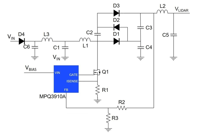
Figure 2: MPQ3910A Block Diagram
2.2 Related Solutions
This reference design is based on the following MPS solution:
| MPS Integrated Circuit | Description |
| MPQ3910A | 5V to 35V input, peak current mode, asynchronous boost controller, AEC-Q100 qualified |
2.3 System Specifications
| Parameter | Specification |
| Input voltage range | 3VDC to 35VDC |
| Output voltage | 300VDC |
| Maximum output current | 15mA |
| Switching frequency | 375kHz |
| Board form factor | 89mmx63mmx5mm |
| Peak Effciiency | 83% |
| 300V output ripple | 200mVP-P |
3 Design
3.1 Schematics

Figure 3: Schematic
3.2 BOM
| Designator | Qty | Value | Package | Manufacturer | Manufacturer P/N |
| C1, C3, C16 | 3 | 0.1µF, 250V | 0805 | TDK | CGA4J3X7T2E104K125AE |
| C2, C4 | 2 | 0.47µF, 250V | 1812 | Murata | GCJ43DR72E474KXJ1L |
| C5 | 1 | 15nF 50V | 0603 | Murata | GCM188R72A153KA37D |
| C6, C8, C9 | 3 | 4.7µF, 50V | 0805 | TDK | CGA4J3X5R1H475M125AB |
| C7 | 1 | 47µF, 50V | 6x6 | Panasonic | EEE-FT1H470AP |
| C10 | 1 | 0.47µF, 450V | 1812 | TDK | C4532X7T2W474M230KE |
| C11 | 1 | 1µF, 50V | 0805 | Murata | GCM21BR71H105KA03L |
| C12 | 1 | 4.7µF, 25V | 0805 | TDK | CGA4J1X7R1E475K125AC |
| C13 | 1 | 0.47µF, 16V | 0603 | Murata | GCM188R71C474KA55D |
| C15 | 1 | 6.8nF 16V | 0603 | Murata | GCM188R72A682KA37D |
| D1, D2, D3 | 3 | BAS21 | SOD-323 | Rohm | BAS21VMFHTE-17 |
| D4 | 1 | NRVTS245ESFT3G | SOD-123 | ON Semiconductor | NRVTS245ESFT3G |
| D5 | 1 | SMBJ30CA-E3/52 | SMB | Comchip | ATV06B240JB-HF |
| D6 | 1 | PMEG6010CEJ | SOD-323 | Nexperia | PMEG6010CEJ,115 |
| L1 | 1 | 12µH, 1.75A | 6235 | Coilcraft | LPS6235-123MRB |
| L2 | 1 | 4.7µH, 0.6A | 0805 | Murata | LQM21PZ4R7NGRD |
| L3, L4 | 2 | 1µH, 1.3A | 0805 | Murata | LQM21PZ1R0NGRD |
| Q1 | 1 | SQJ454EP | SO-8FL | Vishay | SQJ454EP-T1_GE3 |
| R1, R3, R13 | 3 | 0Ω, 5% | 0603 | Vishay Dale | CRCW06030000Z0EB |
| R2, R7, R8, R9, R10 | 5 | 100kΩ, 1% | 0603 | Vishay | CRCW0603100KFKEA |
| R4 | 1 | 6.2kΩ, 1% | 0603 | Panasonic | ERJ-3EKF6201V |
| R5 | 1 | 50mΩ, 1% | 1206 | Panasonic | ERJ-8CWFR050V |
| R6 | 1 | 7.5kΩ, 5% | 0603 | Vishay | CRCW06037K50FKEA |
| R11 | 1 | 82kΩ, 1% | 0603 | Vishay | CRCW060382K0FKEA |
| R12 | 1 | 2kΩ, 1% | 0603 | Vishay | CRCW06032K00FKEA |
| U1 | 1 | MPQ3910 | MSOP-10 | MPS | MPQ3910GK-AEC1 |
3.3 PCB Layout

Figure 4: PCB Layer 1

Figure 5: PCB Layer 2

Figure 6: PCB Layer 3

Figure 7: PCB Layer 4
4 Test Results
4.1 Efficiency and Regulation
VOUT = 300V, L = 12µH, fSW = 375kHz, TA = 25ºC

Figure 8: Efficiency vs. Load Current

Figure 9: Line Regulation

Figure 10: Load Regulation
4.2 Time Domain Waveforms
VIN = 12V, VOUT = 300V, L = 12µH, fSW = 375kHz, TA = 25ºC
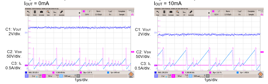
Figure 11: Steady State - Figure 12: Steady State

Figure 13: Start-Up through VIN - Figure 14: Start-Up through VIN

Figure 15: Shutdown through VIN - Figure 16: Shutdown through VIN

Figure 17: Start-Up through EN - Figure 18: Start-Up through EN

Figure 19: Shutdown through EN - Figure 20: Shutdown through EN

Figure 21: Single Load Step - Figure 22: Single Load Step

Figure 23: Repetitive Load Step, 5kHz - Figure 24: Repetitive Load Step, 10kHz

Figure 25: Repetitive Load Step, 20kHz - Figure 26: Repetitive Load Step, 50kHz
Log in to your account
Create New Account