MPQ3426 - Pre-Boost Reference Design, Simple Solution to Cold-Crank Transients

Get valuable resources straight to your inbox - sent out once per month
We value your privacy
1 OVERVIEW
1.1 Description
Start-stop functionality is an expected feature in more and more new car models from any manufacturer. However, this presents a challenge in automotive electronics design, as starting the motor in cold weather can make the battery’s voltage drop as low as 3V. This is called a “cold crank.”
The power stage for most 12V automotive systems consists of a single buck converter that typically regulates the output voltage to 5V or 3.3V. Even if the regulator starts working in low-dropout mode, most circuits can be affected by a dip in the input voltage, and may stop functioning. The electronic control unit (ECU) always starts from the nominal battery voltage of 12V, and it is after start-up that cold-crank transients can occur. Using a pre-boost offers a solution to this problem.
A pre-boost consists of a boost converter connected in series before a buck converter, which raises the voltage when it falls below a certain threshold. This allows the buck converter to have a steady input voltage and correctly regulate its output to a constant level, regardless of transients in the 12V harness. The boost’s bias voltage is provided by the main buck converter, thus extending the operating input voltage of the system to 2V or lower.
This reference design will help engineers designing a pre-boost for a power supply up to 18W.
1.2 Features
- Wide Operating Input Range (from
- 3.5A Continuous Output Current
- 350kHz to 2.5MHz Programmable Switching Frequency
- Low-Dropout Mode
- Over-Current Protection (OCP) with Valley-Current Detection and Hiccup Mode
- Available with Wettable Flank
- High Efficiency Up to 92%
- Reverse Polarity Protection
- Second-Order EMI Filter
- Available in AEC-Q100 Grade 1
- Meets CISPR25 Class 5 EMC Standard

Figure 1: MPS Pre-Boost Reference Design Board
1.3 Applications
- Automotive Infotainment
- Automotive Safety and ADAS
2 REFERENCE DESIGN
2.1 Block Diagram
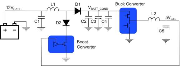
Figure 2: Block Diagram"
In addition to being part of the pre-boost converter, L1 and C1 act as an input filter for conducted EMI. D1 protects the buck converter IC from reverse polarity. D2 is optional to protect the boost IC if no other reverse polarity protection is implemented.
2.2 Related Solutions
This reference design is based on the following MPS solutions:
| MPS Integrated Circuit | Description |
| MPQ3426 | Asynchronous boost converter with 6A of switch current capability and a 3.2V bias voltage |
| MPQ4430 | 36V synchronous buck converter capable of delivering 3.5A |
Table 1: System Specifications
2.3 Systems Specifications
| Parameter | Specification |
| Working input voltage | <2VDC to 36VDC |
| Start-up input voltage | 5VDC to 36VDC |
| Output voltage | 5VDC |
| Maximum output current | 3.5A (at 5V output) |
| Switching frequency | 400kHz |
| Board form factor | 90mmx90mmx10mm |
| Efficiency | >85% |
| 12V output ripple | 15mV |
Table 2: System Specifications
| Lowest Battery Voltage during Cold Crank | Max Output Current at 5V Output Voltage |
| 1.5V | 0.9A |
| 2.0V | 1.2A |
| 2.5V | 1.6A |
| 3.0V | 2.1A |
| 3.5V | 2.8A |
| 4.0V | 3.3A |
| 4.2V | 3.5A |
Table 3: Battery Voltage Transient vs. Output Current
3 TEST RESULTS
3.1 Efficiency
VBATT = 12V, VSYS = 5V, LBOOST = 2.2µH, LBUCK = 4.7µH, TA = 25°C, unless otherwise noted.
With input filter, protection diode, and pre-boost.
Figure 9: Efficiency vs. Load Current - AAM MODE

Figure 10: Efficiency vs. Load Current - CCM MODE
ISYS = 2A, AAM mode

Figure 11: Cold-Crank Transient Voltage (100ms/div)
3.2 EMC Measurements
VBATT = 12V, VSYS = 3.3V, LBUCK = 4.7μH, COUT= 44μF, fSW = 400kHz, TA = 25°C.
150kHz to 108MHz

Figure 2115: CISPR25 Class 5 Conducted Emissions
150kHz to 30MHz

Figure 2216: CISPR25 Class 5 Radiated Emissions
Log in to your account
Create New Account