AN222 - MP5048 Design for Parallel Applications

Get valuable resources straight to your inbox - sent out once per month
We value your privacy
Introduction
This application note discusses the MP5048 design for parallel applications. The MP5048 is a monolithic integrated controller and switch that can be paralleled for higher current applications. The device includes a high-side MOSFET (HS-FET) and circuitry that enable it to operate as a standalone device or to be controlled by a hot-swap controller. It can drive up to 15A of continuous current per MP5048 device. Figure 1 shows the typical application schematic of a single MP5048 device.

Figure 1: MP5048 Standalone Typical Application Schematic
The MP5048 limits the inrush current to the load when a circuit card is inserted into a live backplane power source which limits the backplane’s voltage drop. The device also limits the internal MOSFET current by controlling the gate voltage through the current-limit reference input.
The MP5048 offers many features to simplify the system design including an integrated solution to monitor the output current (IOUT) and die temperature. This eliminates the need for an external current-sense power resistor power MOSFET or thermal sense. The device also detects the power FET gate source and drain short conditions and provides feedback for the controller.
Parallel Applications
To allow currents above the 15A limit the MP5048 can be used in parallel applications. Figure 2 shows a typical application schematic of multiple MP5048 devices connected in parallel.
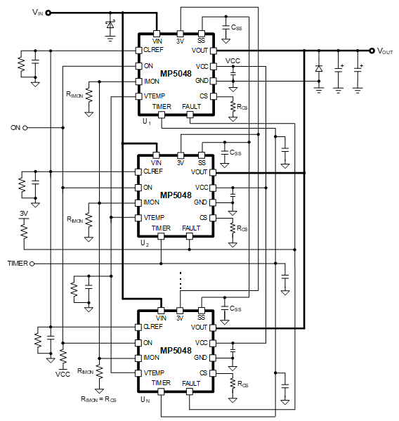
Figure 2: MP5048 Parallel Operation Typical Application Schematic
Table 1 on page 5 shows the pin connections that must be made to enable proper function. Each CS pin must have a separate resistor and cannot be connected together and all CS resistors must have the same resistance.
Table 1 shows the pins of the MP5048 that must be connected together in parallel applications.
Table 1: Required Pin Connections for Parallel Applications
| Pin Name | Required Pin Connections |
| CLREF | Place a resistor on each phase based on the CLREF pin’s normal voltage (VCLREF_NORM) and the current limit (ILIMIT). VCLREF_NORM can be calculated with Equation (1):
$$V_{CLREF\_NORM} = I_{CLREF\_NORM} \times R_{CLREF}$$ Where ICREF_NORM is the CLREF normal current and RCLREF is the CLREF resistor. ILIMIT can be calculated with Equation (2): $$I_{LIMIT} = \frac {V_{CLREF\_NORM}}{(g_{CS} \times R_{CS})}$$ Where gCS is the current-sense gain when the power FET is fully on (typically 25µA/A) and RCS is the CS resistor. In addition place a 1nF to 10nF capacitor between CLREF and AGND. |
| ON | ON All MP5048 devices connected in parallel must connect the ON pins together to ensure the same enable signal. This can be from a logic device or via a resistor divider between the VIN and ON pins. |
| IMON | IMON The IMON pin provides the total current during operation which can be calculated with Equation (3):
$$\text{Total Current} = N \times \text{e-fuse}$$
During start-up IMON balances the soft-start (SS) current between the MP5048 devices. Place a resistor on each phase. Refer to the MP5048 datasheet for more details on calculating RCS.
The equivalent IMON resistance (RIMON) can be calculated with Equation (4): $$R_{IMON} = \frac{R_{cs}} {N}$$ Where N is the number of devices connected in parallel. |
| GND | The GND pin of each MP5048 device must be connected to the same ground reference. |
| VIN | The VIN pin is the high-voltage (HV) input for the e-fuse device. All MP5048 devices connected in parallel must be connected to the same power plane. A TVS protection device is required to prevent the input voltage (VIN) from exceeding the limits specified in the MP5048 datasheet. |
| SS | Place a capacitor between the SS pin and the analog signal ground on each phase. This ensures synchronized soft start during the start-up sequence. |
| VOUT | The VOUT pin of all MP5048 devices connected in parallel must be connected to the same power plane. A Schottky diode is required to be connected between the VOUT and GND pins to provide a high-current freewheeling path during over-current protection (OCP) or short-circuit protection (SCP) conditions. |
| TIMER | Place a capacitor between the TIMER pin and the analog signal ground on each phase. TIMER synchronizes the insertion delay retry delay and OCP timer for all devices connected in parallel. |
Table 2 shows the optional pin connections of the MP5048 that can either be separate or combined.
Table 2: Optional Pin Connections
| Pin Name | Optional Pin Connections |
| VTEMP | Place a minimum 10kΩ resistor and a maximum 1nF capacitor between VTEMP and the analog signal ground. The VTEMP pin of all the MP5048 devices can be connected to obtain the highest device reading or each individual signal can be routed to read the temperature of each e-fuse. |
| VCC | Place 1µF capacitor between VCC and the analog signal ground on each phase. The VCC pin of each e-fuse can be connected together or left as individual connections. |
| 3V | Place a 1µF capacitor between 3V and the analog signal ground on each phase. The 3V pin of each phase can be connected together or left as individual connections. |
| FAULT | The FAULT pin is an open-drain output that can be pulled up via a 10kΩ to 100kΩ capacitor between FAULT and VCC or between FAULT and 3V depending on the voltage level required by the system. FAULT can be left as an individual connection for detailed e-fuse fault monitoring or connected together to obtain a combined fault signal for all e-fuse devices. |
| MODE | MODE sets the e-fuse operation to either hiccup mode or latch-off mode during fault conditions. The MODE pin of all the MP5048 devices can be set individually but all MP5048 devices connected in parallel must have the same MODE setting. The MODE pins can be connected together to set the device’s operation. |
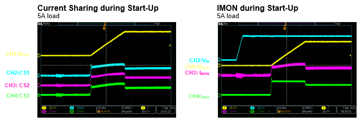
During the start-up sequence current balancing between the MP5048 devices connected in parallel is achieved using the connections of the SS and IMON pins. The SS pin ensures that all MP5048 devices connected in parallel have the same soft-start (SS) ramp rate during the start-up sequence. This provides inherent current balancing between the MP5048 devices as the output voltage (VOUT) rises. If any conditions occur that cause the current to increase in one of the MP5048 devices then an active current-balance loop is activated using the total current from IMON and the individual e-fuse current via the CS pin which balances the current across the MP5048 devices connected in parallel.
In addition to the layout the positive temperature coefficient of the MOSFET resistance (RDS(ON)) helps with current balancing. If one MP5048 device carries more current then the device heats up more and increases its RDS(ON) which forces the current to the other MP5048 devices.
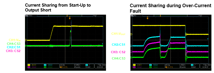
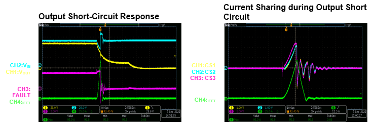
If an overload condition occurs the MP5048 devices connected in parallel regulate to the configured over-current protection (OCP) threshold and the connected TIMER pin begins to charge. Once the voltage on the TIMER pin reaches the trip threshold (0.6V) all the MP5048 devices are disabled and shut down due to the over-current (OC) condition. If the MP5048 devices are set to latch-off mode two methods can be used to clear the fault. The MP5048 remains in the fault state until the power on the ON pin is cycled low and then high again to clear the fault condition and begin a SS turn-on sequence. To clear the fault and perform a full device reset decrease the input voltage (VIN) below 3V for 100ms to trigger the VCC voltage (VCC) under-voltage lockout (UVLO) falling threshold. This causes a full device reset and an insertion delay occurs when VIN is rising.
During a power cycle if VIN does not drop below 3V for 100ms the VCC UVLO falling threshold is not triggered for all MP5048 devices connected in parallel. The MP5048 devices that trigger the VCC UVLO falling threshold enter an initialization mode while the MP5048 devices that have not triggered the VCC UVLO falling threshold remain in normal operation. If the MP5048 devices are in different operational states then the MP5048 devices connected in parallel do not restart properly.
If the MP5048 devices are in hiccup mode TIMER sequences the retry time between all the MP5048 devices connected in parallel. At the end of the retry time the MP5048 devices connected in parallel are re-enabled and a new start-up sequence begins.
To prevent power-on reset (POR) VIN must exceed the 5.25V under-voltage lockout (UVLO) threshold during normal operation.
EV5048-V-00A Evaluation Board
Figure 3 shows the 5-phase EV5048-V-00A. This application note details test results using a 3-phase EV5048-V-00A.
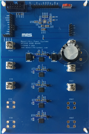
Figure 3: EV5048-V-00A Evaluation Board
Evaluation Board Layout
The EV5048-V-00A evaluation board consists of four layers (see Figure 4 to Figure 7). The top layer for each e-fuse has the same shape to achieve current balancing across all MP5048 devices during steady-state operation.
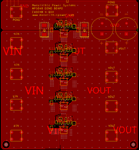
Figure 4: EV5048-V-00A Top Layer
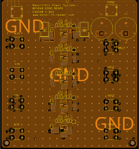
Figure 5: EV5048-V-00A Mid-Layer 1
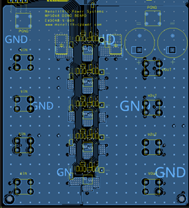
Figure 6: EV5048-V-00A Mid-Layer 2
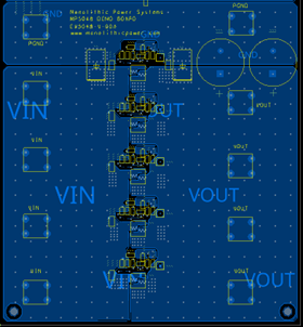
Figure 7: EV5048-V-00A Bottom Layer
Evaluation Board Schematic
Figure 8 shows the EV5048-V-00A evaluation board schematic for the e-fuses.
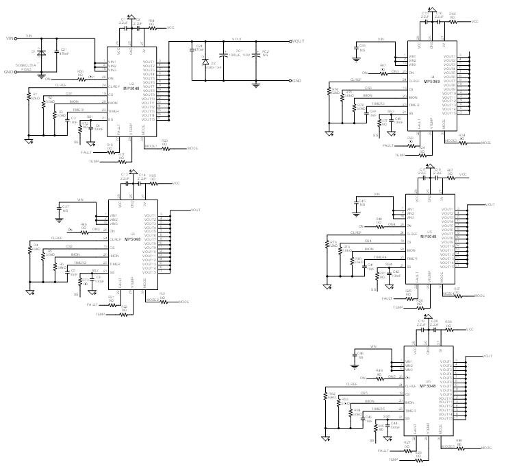
Figure 8: EV5048-V-00A E-Fuse Schematic
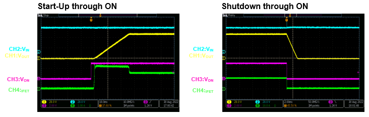
Waveforms
Conclusion
This application note discusses a simple system design using the MP5048 to ensure proper parallel operation. E-fuse designs for parallel applications provide flexibility for the growing demand of higher current circuit protection. The MP5048 is a versatile solution that offers strategic pin connections as well as a positive temperature coefficient to achieve robust circuit protection and current balancing for high-current parallel operation.
_______________________
Did you find this interesting? Get valuable resources straight to your inbox - sent out once per month!
Technical Forum
 Latest activity 13 hours ago
 1 Comment
Latest activity 20 hours ago
1 Comment
Latest activity a day ago
1 Comment
1 Comment
Latest activity 20 hours ago
1 Comment
Latest activity a day ago
1 Comment
Log in to your account
Create New Account