MP2731 USB PD Reference Design: 4.5A, NVDC Single-Cell Charger with OTG
DOWNLOAD THE FULL REFERENCE DESIGN

Get valuable resources straight to your inbox - sent out once per month
We value your privacy
1.1 Description
The MP2731 USB power delivery (PD) reference design provides a complete solution for USB PD applications that comply with USB PD3.0 specifications. The major components of this reference design include the MP2731 — a 4.5A, narrow voltage DC (NVDC) single-cell Li-ion battery charger — and a CCG3PA (USB PD controller).
The reference design offers a bidirectional DRP Type-C port. When a USB input is present, the port functions as an upstream-facing port (UFP) to charge the battery. When a USB PD sink is connected to the Type-C port, the reference design functions as a downstream-facing port (DFP), and can provide a 5V USB On-the-Go (OTG) for the sink device. This reference design provides NVDC architecture with power path management functionality, which makes the solution well-suited for smartphones, tablets, and various portable charging applications.
1.2 Features
- 5V to 16V Operating Input Voltage Range Supporting Common Fixed PDO Voltages
- Up to 22V Maximum Sustainable Voltage
- High-Efficiency, 4.5A, 1.35MHz Buck Charger
- Support USB PD 3.0 and BC 1.2 Protocols
- USB On-the-Go (OTG) Function to Power USB Port from Battery Power
- Up to 9A Battery Discharge Current
- Narrow Voltage DC (NVDC) Power Path Management Functionality
- I2C Interface for Configurable System Parameter Settings
- High-Accuracy: ±0.5% Charge Voltage Regulation, ±5% Charge Current Regulation
- Configurable JEITA Thresholds for Battery Temperature Protection
- Provide Thermal Regulation Loop and Thermal Shutdown Protection
- Input and System Over-Voltage Protection (OVP)
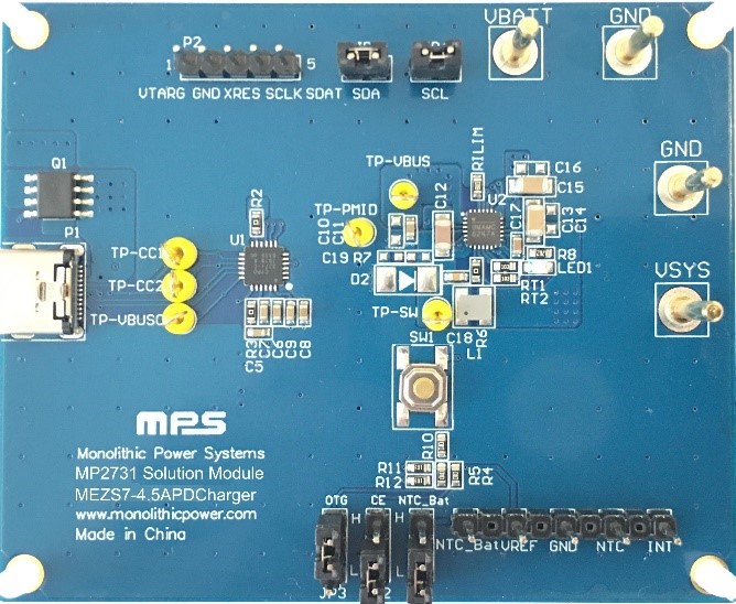
Figure 1: Solution Module for USB PD
1.3 Applications
- Tablets
- Smartphones
- Mobile Devices
Reference Design
2.1 Block Diagram
The MP2731 USB PD reference design offers a cost-effective solution to achieve up to 18W PD fast charging by pairing a highly integrated MP2731 charger with a universal PD controller (CCG3A). A universally available Type-C connector on the board serves as a bidirectional input. The back-to-back input FET configuration is optional because the MP2731 also provides an internal input-blocking FET, which helps to further reduce PCB size and BOM cost (see Figure 2).
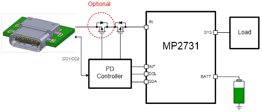
Figure 2: MP2731 USB PD Charger System Block Diagram
2.2 Related Solutions
This reference design is based on the following MPS solution:
Table 1: System Specifications
| MPS Integrated Circuit | Description |
| MP2731GQC-0000 | 4.5A, NVDC single-cell charger with USB On-the-Go (OTG) |
System Specifications
Table 2: System Specifications
| Parameter | Specification |
| Input voltage range | 5 to 16V |
| Charge-full voltage | 4.2V, I2C-configurable |
| Charge current | 3.0A, I2C-configurable |
| Input voltage regulation | 4.6V, I2C-configurable |
| Input current regulation | 0.5A, I2C-configurable |
| OTG voltage regulation | 5.1V, I2C-configurable |
| OTG current limit | 2.4A, I2C-configurable |
| Board form factor | 78mmx63mmx12mm |
| Efficiency | >90% |
Test Results
3.1 Charge Efficiency
VIN = 5V, 9V, or 12V, VBATT = 3.8V, RL_DCR = 21mΩ, not including the external blocking FET (Q1, Q2)Image 3
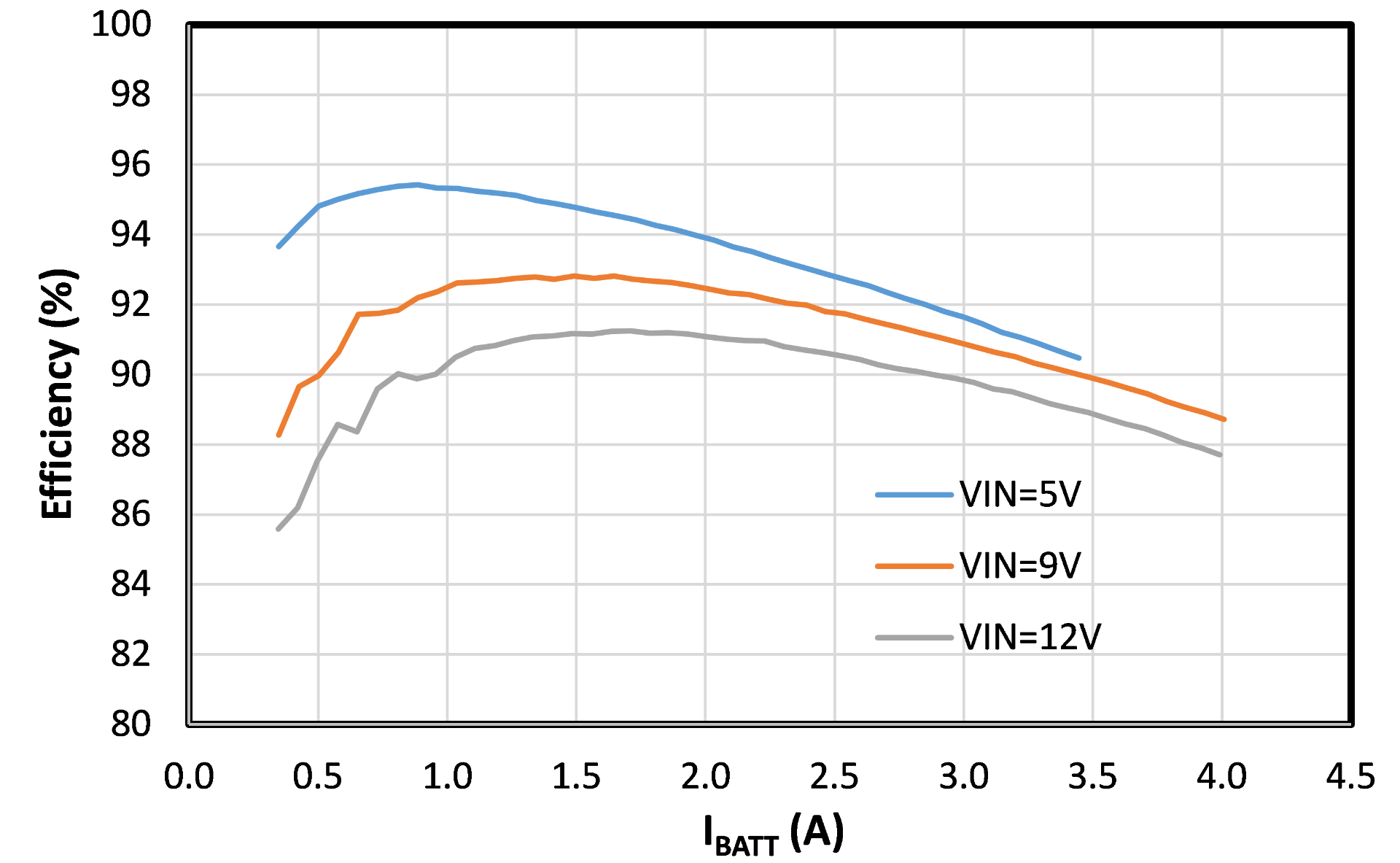
Efficiency vs. Charge Current
3.2 Thermal Measurements
Conditions: VIN = 12V, VBATT = 3.8V, IBATT = 3A, TA = 24°C.
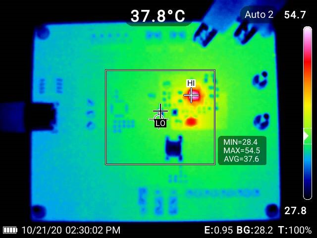
Figure 6: Thermal Performance
Log in to your account
Create New Account