Smart Plug Reference Design - MP161 Non-Isolated Buck Regulator with ESP8266

Get valuable resources straight to your inbox - sent out once per month
We value your privacy
1 OVERVIEW
1.1 Description
Nowadays everything is connected. So why not also connect the wall plugs? MPS presents a reference design with the MP161 part that will allow customers to join the IoT market. This is a two boards product, one for the DC/DC converter and the relay and the other for the Wi-Fi module. The configuration is designed to fit into a wall-plug.
1.2 Features
- Integrated IC supply solution (12V + 3V3 + Relay Driver)
- Wi-Fi 802.11 b/g/n (HT20) protocol
- 35.4 mW active input power under stand-by operation
1.3 Applications
IoT non-isolated designs

REFERENCE DESIGN
2.1 Block Diagram

Figure 1: Block Diagram
2.2 Related Solutions
This reference design is based on the following MPS solutions:
| MPS Integrated Circuit | Description |
| MP161B-33 | High voltage buck regulator |
2.3 System Specifications
| Parameter | Specification |
| Input Voltage Range | 90 V to 265 V AC |
| Output Voltage | 12 V ± 1.5% DC |
| Nominal Load | 12 V / 17.5mA, 3.3V / (70 mA for T1 – 250 mA for T2) |
| Peak Output Current | 270 mA (at 12V output) |
| Output Voltage of LDO | 3.3 ±1.5% V |
| Output Current of LDO | 70 – 250 mA |
| Switching Frequency | 40 kHz (under nominal conditions) |
| Board form factor | 50 x 50 x 30 mm |
| Efficiency | > 90 % |
| 12V output ripple | 17 mV (under nominal conditions) |
| Wi-Fi protocol | 802.11 b/g/n (HT20) ESP8266 based |
2.4 MP161: Integrated non-isolated Buck Regulator
The MP161 integrates a 700V switching regulator, a low-dropout linear regulator and two channel relay drivers. The MP161 also has a special standby mode to minimize standby power. The MP161 is designed for home automation, industrial automation, and any other applications that adopt relays and MCUs.
Features
- Integrated 700V MosFET and current source
- Constant voltage regulation with internal loop compensation
- Optimized light-load efficiency by frequency modulation
- Standby mode
- Anti-audible noise operation by peak current modulation
- Adjustable or fixed 12V Output
- Low operating current
- Over-Temperature Protection (OTP), Short-Circuit Protection (SCP), Over-Load Protection (OLP) and Over-Voltage Protection (OVP)
Relay Driver
- 2 Ω On state resistance
- Rail voltage up to 30V
- Integrated freewheeling diode
- Nominal off driver
Low-Drop Out (LDO) lineal regulator
- Up to 30V input voltage
- Fixed output, with 3V3 and 5V options
- Over-Temperature Protection (OTP)

Figure 2: Internal block diagram of the MP161"
3 DESIGN
3.1.1 Inductor Selection
The MP161 has a minimum off-time, 9.5 or 12 us depending on the IC variant A or B/C, that determines the maximum output power. With eq. 1 we can estimate the Over Load Point (OLP) under Continuous Conduction Mode (CCM)
With 1 mH inductor we can guaranty the output power 3.3W, taking the tolerance into consideration.
$$P_{o\;max}=V_o \left(I_{L\;limit} - {V_oτ_{min\;off}} \over 2L \right)$$3.1.2 Output Capacitor
We choose the output capacitor in order to fulfil the ripple requirement. In this case is 150mV.
With eq.2 we can estimate the voltage ripple under CCM: 33 mV with 100uF
$$V_{out\;ripple}=\frac{\Delta_i}{8f_s C_o }+\Delta_i R_{ESR}$$3.2 Wi-Fi module consumption
The Wi-Fi module consumption is described in the figure below. This periodic load profile will be considered as nominal load condition (table 1). Where: T1 is 97 ms, T2 is 1.5 ms and T is T1+T2.

Figure 3: Block diagram
3.3 Schematic
This board is divided in two schematic files in order to separate the power stage (figure 4) and the communications (figure 5) one.
")
Figure 4: Power stage (Rectifier + DC/DC)

Figure 5: Wi-Fi module
3.4 BOM
| Qty. | Designator | Manufacturer PN | Manufacturer | Value |
| 7 | C1, C4, C5, C6, C7, J1, J2 | NS | ||
| 7 | J4, J8, R1, R4, R6, R9 | NS | ||
| 1 | C2 | 1206 220nF | 220nF | |
| 1 | C3 | 0603 47pF | 47pF | |
| 1 | C8 | 0603 1uF 25V | 1u 25V | |
| 1 | C9 | 860021373005 | Wurth | 3.3uF 400V |
| 1 | C10 | 1206 1uF | 1uF | |
| 1 | C11 | EKRG250ETD101MF09D | United Chemi-Con | 100uF 25V |
| 1 | C12 | F861BG224M310C | KEMET | F861BG224M310C |
| 1 | C14 | 1206 100nF | 100nF | |
| 2 | D1, D3 | RS1J | DIODES | RS1J |
| 1 | D2 | DF04S-T | Diodes Incorporated | DF04S-T |
| 1 | F1 | 3403.0156.24 | Schurter | 0.1 A / 250 VAC |
| 1 | L1 | DR0608-105L | Coilcraft | DR0608-105L |
| 1 | L2 | RLB0914-102KL | BOURNS | 1mH 0.3A |
| 2 | R2, R12 | 0603 0R | 0R | |
| 1 | RL1 | PE014012 | OEG - TE CONNECTIVITY | PE014012 |
| 1 | U1 | MP161B-33 | Monolithic Power Systems | MP161 |
| 1 | VAR1 | B72660M0271K072 | EPCOS | B72660M0271K072 |
Table 3: Bill of materials for the Power Stage
| Qty. | Designator | Manufacturer PN | Manufacturer | Footprint | Value |
| 1 | C1 | 1206 100nF | 1206 | 100nF | |
| 7 | D1, J1, J2, J3, Q1, Q2, R1 | NS | |||
| 7 | R2, R4, R5, R6, R9, R13, R17 | NS | |||
| 1 | J4 | JS202011SCQN | C&K | DIP-SWITCH | JS202011SCQN |
| R3, R12, R14 | 0603 0R | 0603 | 0R | ||
| R7, R8, R10, R11, R16, R18 | 0603 10k | 0603 | 10k | ||
| 1 | R15 | 1206 0R | 1206 | 0R | |
| 2 | S1, S2 | FSMSMTR | TE Connectivity | TE FSM6JSMA | FSMSMTR |
| 1 | U1 | ESP-12S | RF-Solutions | ESP8266 ESP-12-S | ESP-12S |
Table 4: Bill of materials for the ESP8266 PCB
3.5 PCB Layout
order to deliver a compact solution, we have divided the system into different boards, one for the power stage (figure 4) and the other for the Wi-Fi module (figure 5). These topics should be taken into account once routing this type of solutions we have:
- Even this is a non-isolated high voltage converter, it doesn’t mean that we don’t have to care about distance between traces. We have AC in this board (90-265 Vac) so it is recommended to leave 2.5mm between L and N, also 1.2mm between high and low voltage.
- We have high dV/dt voltage nodes and high dI/dt currents in the power loop so the use of decoupling capacitors is a must.


Figure 6: PCB Power bottom layer (blue) and top layer (red)


Figure 7:PCB ESP8266 bottom layer (blue) and top layer (red)
4 TEST RESULTS
4.1 Time Domain Waveforms

Figure 8: Input current and voltage. (Nominal Load)

Figure 9: Diode anode-cathode voltage.(Vin 265Vac, Vo 12V, Io 270mA (SW Figure1))

Figure 10: Output voltage and LDO. (Nominal Load)

Figure 11: Load behaviour. (Nominal Load)

Figure 12: LDO voltage ripple. (Nominal Wi-Fi Load)

Figure 13: Normal operation consumption. (Nominal Load)

Figure 14: Stand-by operation consumption. (Stand-by-Load)
4.2 Thermal Measurements
| Author | Oriol Cos |
| Facilities | MPS Barcelona |
| Date | May 14, 2019 |
| Environmental Conditions | 25ºC / 31% / 1013 hPa |
| IC | MP161B-33 |
| EVM | - |
| Topology | Buck |
| Customer | - |
| Standard | EN50011 |
| Electrical Conditions | Nominal Conditions |
| Test Equipment | LISN: HM6050-2 |
| Spectrum Analyser: R&S FPC1500 | |
| Software: Elektra v2.20 |
| EN5001 | ||||
| Detector | Class | Frequency [MHz] | Limit [dBµV] | |
| Quasi peak | B | 0.15 - 0.5 | 65-55 | |
| 0.5 - 5 | 45 | |||
| 5 - 30 | 60 | |||
| Peak | B | 0.15 - 0.5 | 55 - 45 | |
| 0.5 - 5 | 45 | |||
| 5 - 30 | 50 | |||
| PORT | RESULT | DETECTOR | CLASS | |
| INPUT | L | Passed | Pk, Qp | B |
| N | Passed | |||
Results Details
Results are far enough from the limits to confirm that the board can pass the standard.

Figure 16: System Set Up
4.3.1 Input port: Live (L)

Figure 17: Live conducted emission spectrum
4.3.2 Input port: Neutral (N) 
Figure 18: Neutral conducted emission spectrum
Start-Up

Figure 19: System components
Please follow the steps below to quick start the system.
- Pre-set the AC power supply to 90 VAC ≤ VIN ≤ 265 VAC.
- Turn the power supply off
- Modify the Wi-Fi credentials to allow the module access the router (Figure 20).
- Connect the board and the PC with an FTDI 232-TTL converter interface (Figure 21).
- If the interface is 5V, do not connect pin 3 (VCC) because the Wi-Fi module will be damaged. In this case turn on the AC power supply to program the device. The 3V3 will be generated by the internal LDO
- Otherwise (3V3 output) the PC will supply the module and you can connect the VCC pin.

Figure 20: Wi-Fi credentials
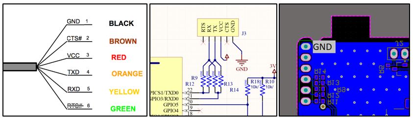
Figure 21: RX-TX Interface
- Open the terminal and program the ESP8266 module. Once the process finishes (Figure 22) the module will send the IP address trough the communication port (Figure 23).
- Then you can go to your browser with this IP and interact with the relay (Figure 24).
5.1 Web Layout
web page interacts directly with the ESP8266 module. The module is connected with the integrated driver on the MP161 so once the user hits the button “GPIO 5” the relay will change their state.

Figure 24: Web Layout
Log in to your account
Create New Account