IOUT
mEZDPD4506AS
PROGRAMMABLE
EOL

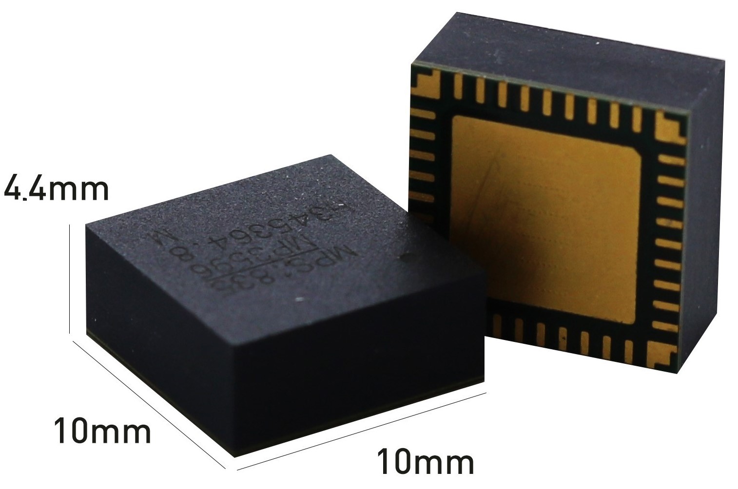
The mEZDPD4506AS is a configurable DC/DC step-down power module up to 6A and 4-45V input voltage. This part has a multiple time programmable memory and a simple GUI to program. Comes in a convenient 10mmx10mmx4.4mm LGA.
Session popupval
Session textval
Session Titefor popup
Session textval
Session Titefor popup
Show default content
Generating Custom Datasheet
Waveforms of Your Custom Specs
- Start Up
- Steady State
- Load Transient
- Vin Shutdown
- SCP
- Line Transient
- Bode Plot
- Efficiency
- BOM
0%
Generating Custom Datasheet...
Loading Design Model...
Choose Your Output Voltage, Your Module Delivered in 7 days
Feeling lucky? Simulate waveforms by viewing datasheet Show me how
| Step 1: | Input your custom specs & View Custom Datasheet |
|
|||||||||||||||||||||||||||||||
|---|---|---|---|---|---|---|---|---|---|---|---|---|---|---|---|---|---|---|---|---|---|---|---|---|---|---|---|---|---|---|---|---|---|
| Step 2: | Save Design to Your Account | ||||||||||||||||||||||||||||||||
| Step 3: | Order your custom evaluation board or module. 7 Day Delivery | ||||||||||||||||||||||||||||||||
Vo Ripple: mV
Vo pk-pk: mV @ △Io= A with slew rate 1.6V/us
Target Efficiency: %
Vo pk-pk: mV @ △Io= A with slew rate 1.6V/us
Target Efficiency: %
Frequency=
Gain=
Phase=
Load Current= Efficiency= Power Loss=
Time= Vsw= Vin= Vo= IL= PG= Io=
| Result: | Bandwidth: kHz | Phase Margin: degree |
|
Select a Performance Characteristic to See Results.
My Designs
| Vin: | V | |
| Io: | A |
| Vin: | V | |
| Io: | A |
| Vin: | V | |
| Io: | A |
| Low Current: | A | |
| High Current: | A | |
| Vin: | V | |
Slew Rate: A/us
| Vin: | V |
| Low Voltage: | V | |
| High Voltage: | V | |
| Io: | A | |
Slew Rate: V/us
Notes: For detailed circuit, including the BOM of mEZDPD4506AS, please see the datasheet. Powered by module MPM3596 which includes IC# DIY8886.
Virtual Bench Summary mEZDPD4506AS

 html2canvas
AAM
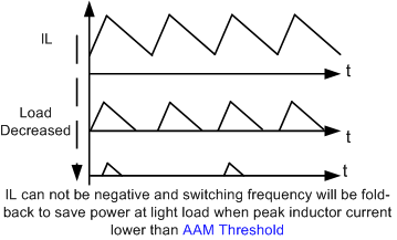
Forced CCM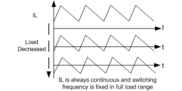
Forced CCM
Vin On/Off
Current Limit Only
Hiccup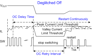
Latch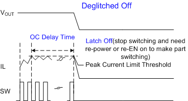
Hiccup
Latch
Discharge
Hiccup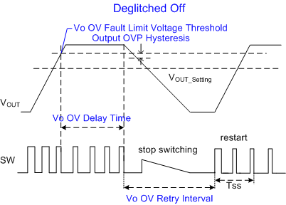
Ignore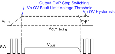
Latch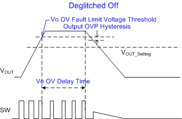
Hiccup
Ignore
Latch
Hiccup
Ignore
Latch
Ignore
Latch
Are you sure to delete the configuration?
New design is created, your previous design is still available in your library.
This will revert your current design to the last saved design. Proceed?
Going to make a new copy.
Your session has expired, please login to continue Customize Your Part & Simulate.
Custom Design
Note: Save design to assign PN
Design Name
PRELIMINARY SPECIFICATIONS SUBJECT TO DESIGN FINALIZATION
DESCRIPTION
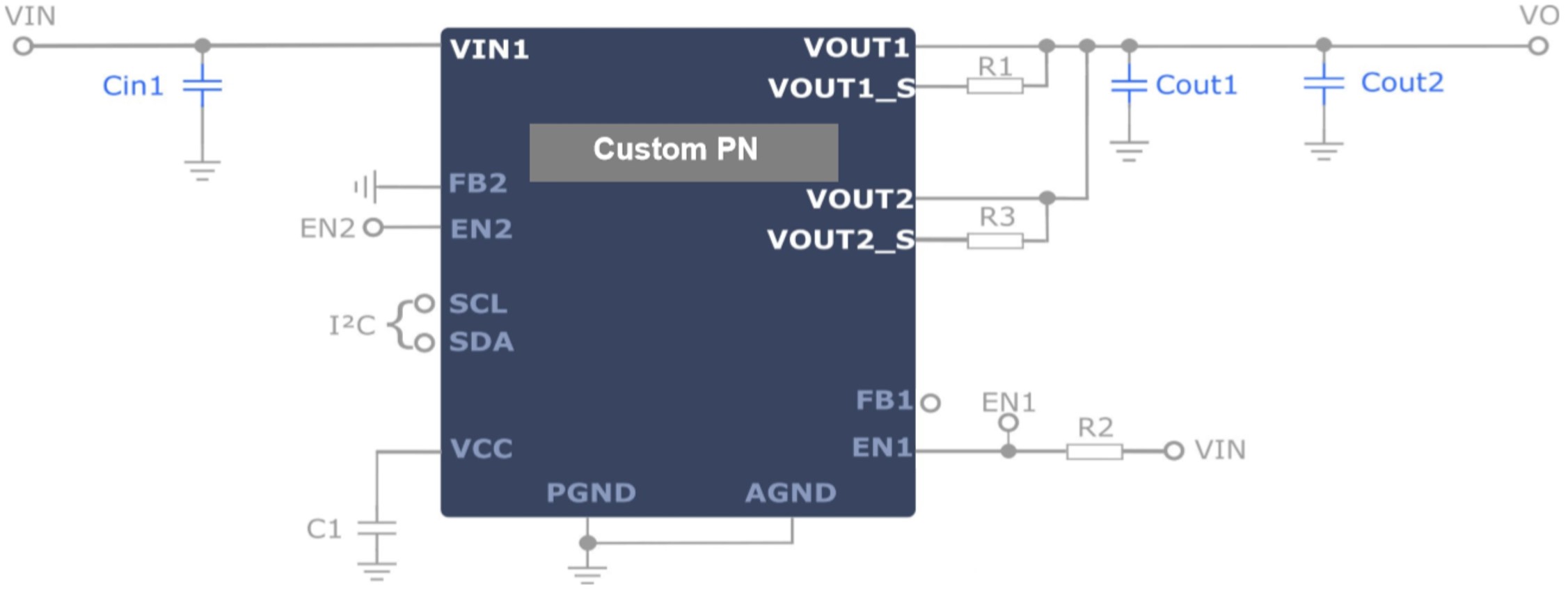
This device is a dual-phase, high-frequency, synchronous, stepdown power module with a PMBus control interface and configured for single output. It integrates internal high-side and low-side power MOSFETS and inductor with high efficiency, and is available in a LGA45 (10mmx10mmx4.4mm) package. With internal compensation network, this device offers a compact solution with a minimal standard external components.
SPECIFICATION OVERVIEW
VOUT
Typical VIN
VIN Min
VIN Max
FEATURES
- Telemetry Readback Includes VIN, VOUT, IOUT, Temperature, and Faults
- Noise-Cancelling, Dual-Side Input Capacitors and Frequency Spread Spectrum Option for Low EMI
- Power Good and Fault Indication
- Output Over-Voltage, Under-Voltage, Over-Current, and Over-Temperature Protection
- 1% VOUT Accuracy Over Operation Temperature Range
- Available in an LGA-45 (10mmx10mmx4.4mm) Package
EFFICIENCY
VIN = , VOUT = , IOUT =
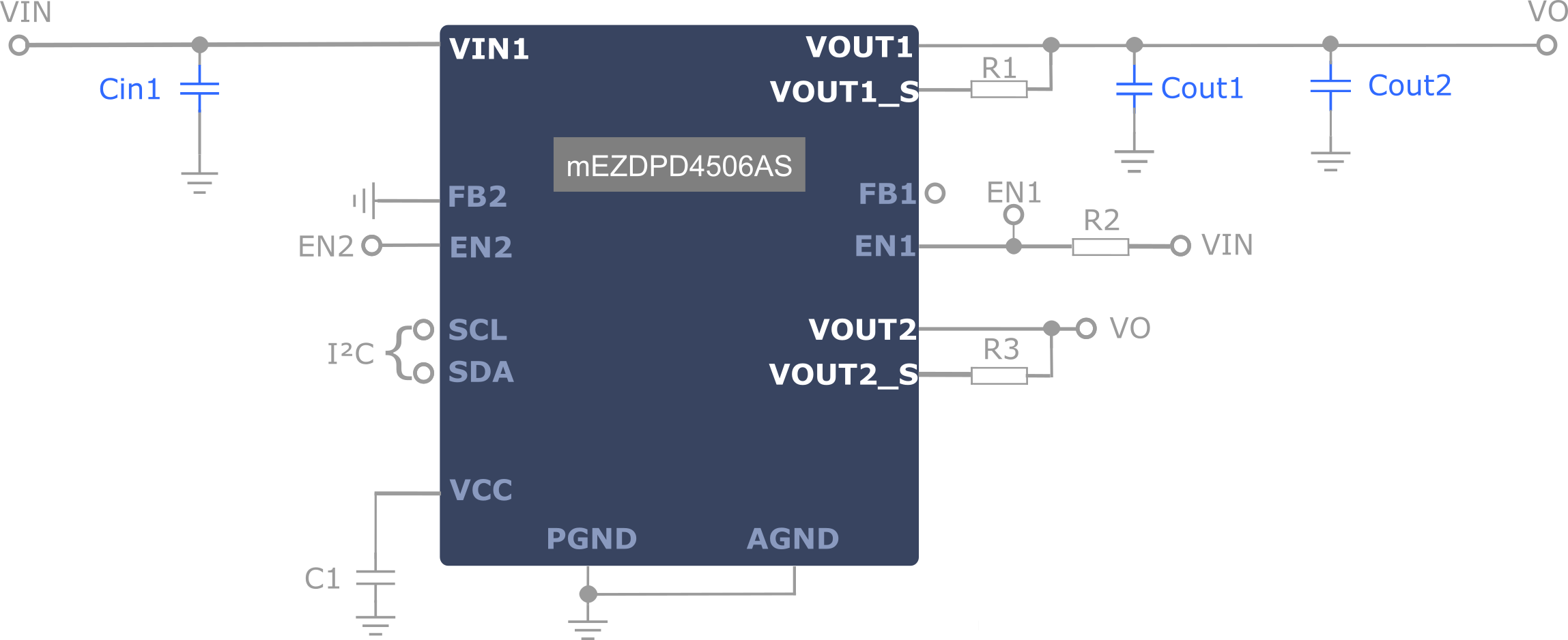
TYPICAL APPLICATION
BOM
Reference
Quantity
Value
Description
Package
Manufacturer
Part Number
Cin1
Cout1
Cout2
R2
1
499kΩ
Film Res, 1%
'0402'
R1
1
10Ω
Film Res, 1%
'0402'
R3
1
10Ω
Film Res, 1%
'0402'
C1
1
1uF
Cap, Ceramic, 10V, X5R
'0402'
U1
1
-
Programmable 45V DC/DC Power
module supply up to 6A
'LGA
(10x10x4.4mm)'
MPS
ORDERING INFORMATION
Part Number
Finalize Design to Order
PACKAGE REFERENCE
OTHER ORDERING OPTIONS
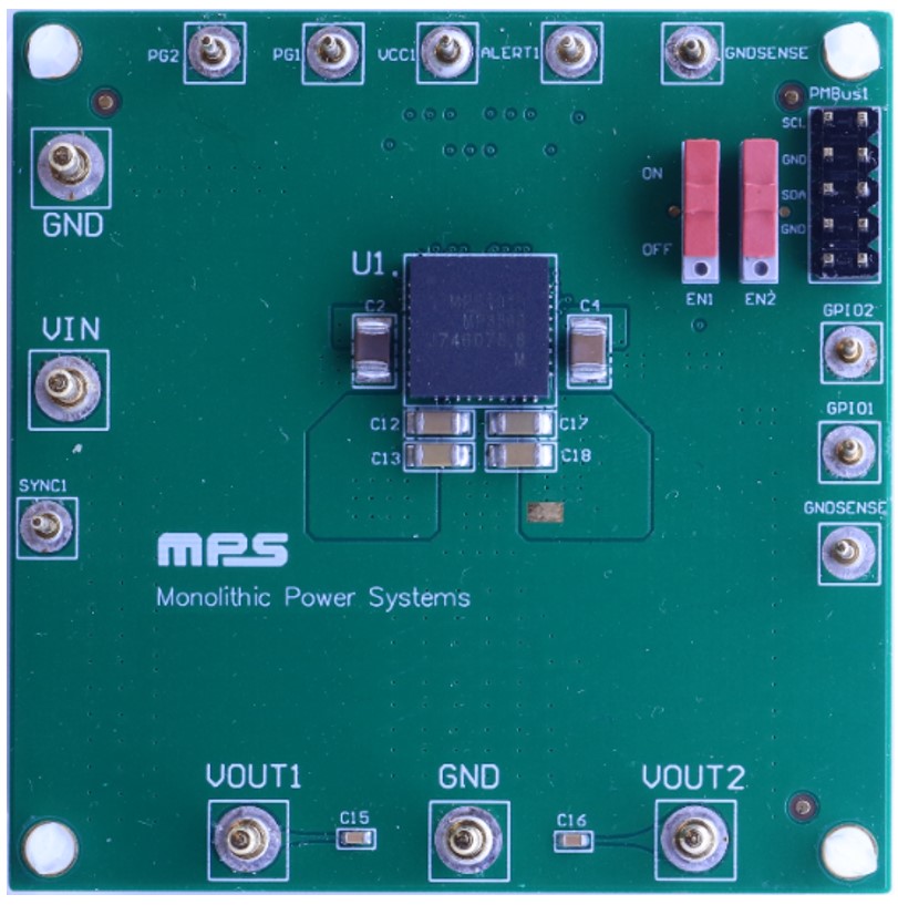
Evaluation Board for Surface Mount Device
The evaluation board is designed to demonstrate the capabilities of your custom MPS Custom PN.
The EVB device is programmed with custom configuration.
Part Number
EVmEZDPD4506AS-00A
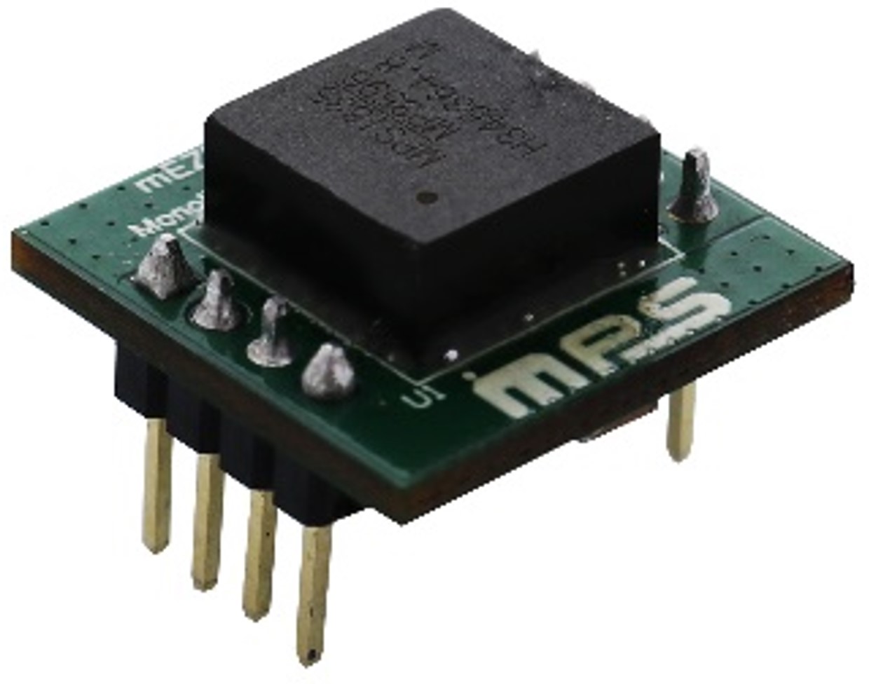
DIP Mount (Pin Out Version)
The Custom PN is your custom device on a DIP mount for an easy-to-use, plug-and-play form factor.
The pin out module device is programmed with custom configuration.
Part Number
mEZDPD4506A
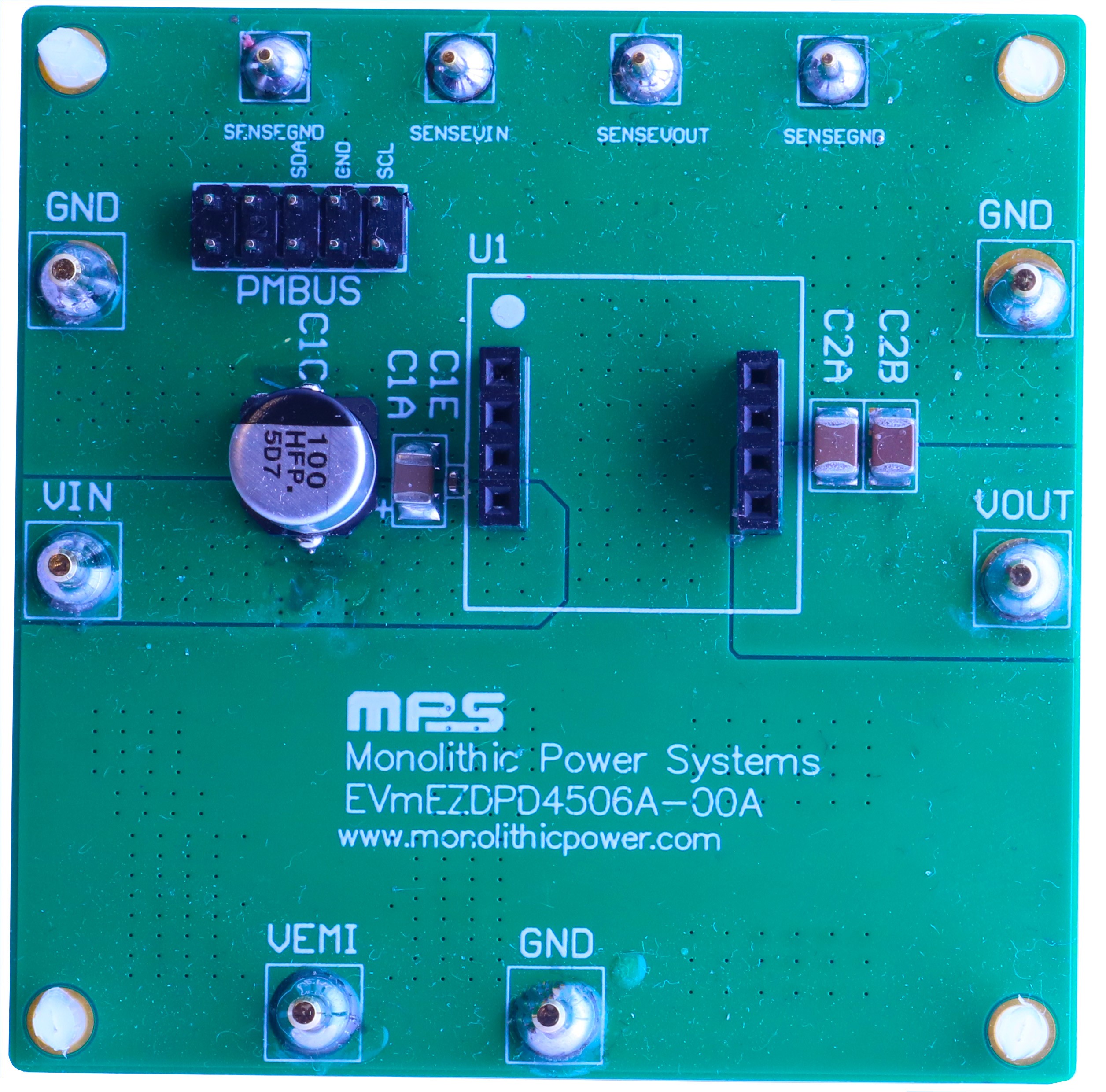
Socket Evaluation Board for DIP Mount
DIP mount socket only. For easy evaluation of pin out module.
Part Number
EVmEZDPD4506A-00A
All EVB schematic and layout files can be found at:
https://www.monolithicpower.com/mezdpd4506as.html
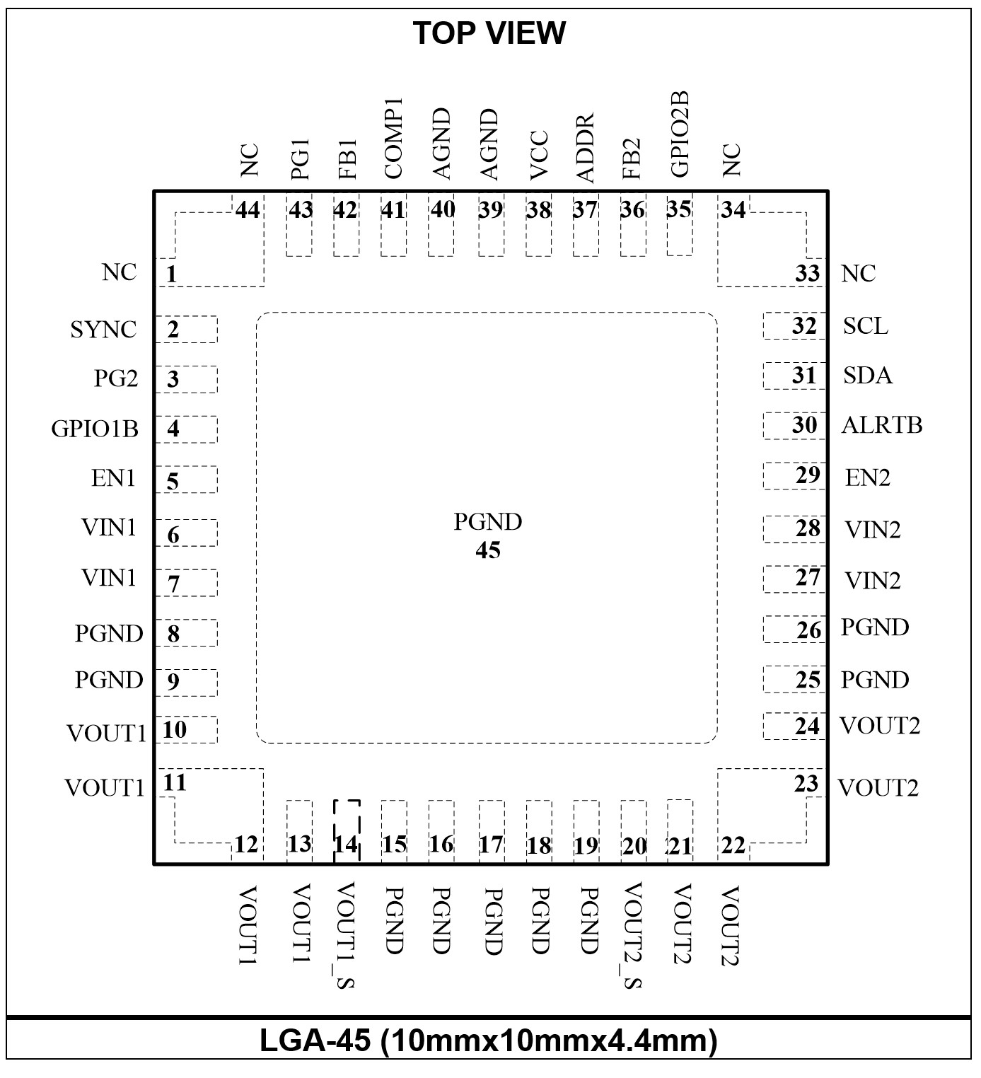
PIN FUNCTIONS
Pin #
Name
Description
1, 33, 34, 44
NC
No connection.
2
SYNC
Synchronized to external clock signal. Can be programmed by PMBus to sync input or sync output.
3
PG2
Power good indicator for channel 2. The output of PG is an open drain. Connect a resistor to a pull-up power source if used.
4
GPIO1B
General I/O port 1.
5
EN1
Enable 1 pin. Drive EN1 high to turn on channel 1, and drive it low or float it to turn off the device. It has an internal, 1MΩ, pull-down resistor to ground.
6, 7
VIN1
Channel 1 supply voltage. This pin supplies all power to the converter. Place a decoupling capacitor to ground as close as possible to the IC to reduce switching spikes. Connect using a wide PCB trace.
8, 9, 15, 16, 17, 18, 19, 25, 26
PGND
Power ground. Reference ground of the regulated output voltage. Connect these pins to large copper areas to the negative terminals of the input and output capacitors.
10, 11, 12, 13
VOUT1
Channel 1 power output. Connect load to VOUT1. An output capacitor is needed.
14
VOUT1_S
Channel 1 power output sense input. Connect directly to VOUT1.
20
VOUT2_S
Channel 2 power output sense input. Connect to VOUT2 directly.
21, 22, 23, 24
VOUT2
Channel 2 power output. Connect load to VOUT2. An output capacitor is needed.
27, 28
VIN2
Channel 2 supply voltage. This pin supplies all power to the converter. Place a decoupling capacitor to ground as close as possible to the IC to reduce switching spikes. Connect using a wide PCB trace.
29
EN2
Enable 2 pin. Drive EN2 high to turn on channel 2, and drive it low or float it to turn off the device. It has an internal, 1MΩ, pull-down resistor to ground.
30
/ALERTB
PMBus alert.
31
SDA
PMBus serial data.
32
SCL
PMBus serial clock.
35
GPIO2B
General I/O port 2.
36
FB2
Error amplifier feedback inputs for channel 2. This pin receives sensed voltage feedback voltage for channel 2 from an external resistive divider across the output. In multi-phase mode, this pin must be pulled up high to disable this channel’s error amplifier.
37
ADDR
Address setting for the PMBus.
38
VCC
Internal 5V LDO regulator output. Decouple with a 0.22µF capacitor.
39, 40
AGND
Signal ground. Ground for internal logic and signal circuit. AGND is not internally connected to power ground. Be sure to connect AGND to power ground in PCB layout.
41
COMP1
Channel 1 error amplifier output. For multi-chip, multi-phase applications, connect this pin for each chip for current sharing.
42
FB1
Error amplifier feedback inputs for channel 1. This pin receives sensed voltage feedback voltage for channel 1 from an external resistive divider across the output.
43
PG1
Power good indicator for channel 1. The output of PG is an open drain. If used, connect a resistor to a pull-up power source.
ABSOLUTE MAXIMUM RATINGS
(1)VIN
-0.3V to +48V
VEN
-0.3V to +45V
All other pins
-0.3V to +6V
Continuous power dissipation (TA = 25°C) LGA-45 (10mmx10mmx4.4mm) (2)
TBD
Junction temperature
150°C
Lead temperature
260°C
Storage temperature
-65°C to +150°C
Supply voltage (VIN)
3.5V to 45V
Output voltage (VOUT)
0.6V to 22V
Operation junction temp (TJ)
-40°C to +125°C
Thermal Resistance (3)
θJA
θJC
LAG-45 (10mmx10mmx4.4mm)
TBD
TBD °C/W
Notes:
- 1) Exceeding these ratings may damage the device.
- 2) The maximum allowable power dissipation is a function of the maximum junction temperature TJ (MAX), the junction-to-ambient thermal resistance θJA, and the ambient temperature TA. The maximum allowable continuous power dissipation at any ambient temperature is calculated by PD (MAX) = (TJ (MAX) - TA) / θJA. Exceeding the maximum allowable power dissipation will cause excessive die temperature, and the regulator will go into thermal shutdown. Internal thermal shutdown circuitry protects the device from permanent damage.
- 3) Measured on JESD51-7, 4-layer PCB.
PROGRAMMABLE ELECTRICAL CHARACTERISTICS
Parameter
Symbol
Description
Min
Typ
Max
Units
Under-Voltage Lockout (UVLO)
VIN UVLO rising threshold
VINUVVTH RISE
Programmed value, device powered on voltage assuming that EN is active
V
VIN UVLO falling threshold
VINUVVTH FALL
Programmed value, device powered off voltage assuming that EN is active
V
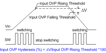
VIN UVLO hysteresis
VINUVHYS
Programmed value, VINUVVTH RISE - VINUVVTH FALL
V
EN voltage hysteresis
VEN HYS
Programmed value
mV
Input Over-Voltage Protection
Input OVP threshold
VINOVP TH
Programmed value, threshold for input over-voltage fault detection
V
Input OVP hysteresis
VINOVP HYS
Programmed value
mV
Input OVP retry interval
Programmed value, restart interval time after triggering input over-voltage fault
ms
Output Voltage
Operation V
V
Programmed value, set value of output voltage
V
Voltage feedback divider range
Programmed value, sets the internal voltage divider ratio
Output voltage margin high
VOUT MARGIN HIGH
Programmed value, output voltage high margin
V
Output voltage margin low
VOUT MARGIN LOW
Programmed value, output voltage low margin
V
Output voltage max
VOUT MAX
Programmed value, upper limit on the output voltage the converter can command regardless of any other commands or combinations
V
Output voltage transition rates
Programmed value, VOUT changing slew-rate control bits, this control only works after SS finishes and during the SS period, the VOUT slew rate is controlled by the SS pin
V/ms
Switching
Switching frequency
fSW
Programmed value, the set value of the switching frequency
kHz
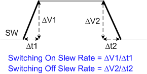
Switching on slew rate (5)
Programmed value, switching rising slew rate
V/ns
Switching off slew rate (5)
Programmed value, switching falling slew rate
V/ns
Dithering cycle
Programmed value, frequency of dithering
kHz
Dithering range
Programmed value
kHz
Soft Start
Soft-start time
tSS
Programmed value, time from the moment when the output starts to rise to when the output voltage reaches the regulation point
ms
tON delay
tON_DELAY
Programmed value, the time from the moment EN turns on to when the output voltage starts rising
ms
tOFF fall
tOFF_FALL
Programmed value, the time from when the output starts to fall until the voltage reaches the zero point
ms
tOFF delay
tOFF_DELAY
Programmed value, the time from the moment EN turns off to when the output starts to fall
ms
Light-Load Mode
AAM threshold for extending frequency
Programmed value, extending frequency if the inductor peak current is below this threshold
mA
AAM threshold for blanking clock
Programmed value, blanking the internal clock if the inductor peak current is below this threshold
mA
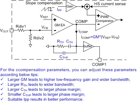
Compensation
Compensation RTH
RTH
Programmed value, compensation resistor RTH
kΩ
Compensation CTH
CTH
Programmed value, compensation capacitor CTH
pF
Compensation CTHP
CTHP
Programmed value, compensation capacitor CTHP
pF
Compensation Slope
Programmed value, slope compensation amplitude
A
Compensation GM
GM
Programmed value, transconductance of the error amplifier
μA/V
Over-Current Protection
Peak current limit
IPEAK-LIMIT
Programmed value, threshold of the inductor peak current limit
A
Valley current limit
IVALLEY-LIMIT
Programmed value, threshold of the inductor valley current limit
A
Over-current retry interval
Programmed value, restart interval time after triggering over-current fault and shutdown
ms
Over-current delay time
Programmed value, device response delay time when output over-current fault is triggered
μs
Output Over-Voltage and Under-Voltage Protection
Output Over-Voltage and Under-Voltage Protection
VOVP_TH
Programmed value, threshold for output over-voltage fault detection, as percentage of VOUT set
%
Output OVP hysteresis
VOVP_HYS
Programmed value, as percentage of VOUT set
%
Output OVP retry interval
Programmed value, restart interval time after triggering output over-voltage fault and shutdown
ms
Output OVP delay time
Programmed value, device response delay time when output over-voltage fault is triggered
μs
Output UVP threshold
VUVP_TH
Programmed value, threshold for output under-voltage fault detection, as percentage of VOUT set
%
Output UVP hysteresis
VUVP_HYS
Programmed value, as percentage of VOUT set
%
Output UVP retry interval
Programmed value, restart interval time after triggering output under-voltage fault and shutdown
ms
Output UVP delay time
Programmed value, device response delay time when output under-voltage fault is triggered
μs
Thermal Protection
Thermal shutdown (5)
TSD
Programmed value, threshold for thermal over-temperature fault detection
°C
Thermal shutdown hysteresis (5)
TSD_HYS
Programmed value
°C
Note:
5) Not tested in production. Guaranteed by design and characterization.
PROGRAM OPERATION SETTINGS
Name
Selected Mode
Description
Note
Output Voltage
Output voltage set mode
0: Use external voltage divider
1: I2C programmable mode
Output voltage bias enable
0: Disable
1: Enable
Switching
Switching dithering Enable/Disable
Frequency dither function enable bit.
0: Disable
1: Enable
Light-Load Mode
Light-load mode
0: AAM
1: CCM
Input Over-Voltage Protection
Input OVP mode
00: Ignore. The device will operate without interruption.
01: Not supported.
10: Immediate off. The device will shut down immediately, and responds according to the Input OVP Retry Settings
Input OVP retry settings
0: No restart
1: Restart continuously
Over-Current Protection
Over-current response
00: Current limit only
01: Deglitched off
10: Immediate off
Over-current retry settings
0: Latch off
1: Restart continuously
Output Over-Voltage and Under-Voltage Protection
Output OVP mode
00: Ignore
01: Deglitched off
10: Immediate off
11: Discharge mode
Output OV retry settings
0: Latch off
1: Restart continuously
Output UVP mode
00: Ignore 01: Deglitched off 10: Immediate off
Output UVP retry settings
0: Latch off
1: Hiccup mode
SYNC IN/OUT
0: SYNC OUT
1: SYNC IN
Power Stage Set
Power stage select
1: Set from MTP
Power stage
001: Dual-phase single output operation
10: Two-chip, 4-phase, 12A operation (master1)
101: Two-chip, 4-phase, 12A operation (master2)
011: Two-chip, 4-phase, 12A operation (slave1)
111: Dual-output buck operation
Rail Address
Enable rail address
0: Disable
1: Enable
Address
Rail Address
GPIO
Input over-voltage
Input over-voltage indication setting
0: Disable
1: Enable
Over-temperature
Over-temperature indication setting
0: Disable
1: Enable
Output under-voltage
Output under-voltage indication setting
0: Disable
1: Enable
Over-voltage
Over-voltage indication setting
0: Disable
1: Enable
Over-current
Over-current indication setting
0: Disable
1: Enable
GPIO mode
GPIO mode set
0: Analog input
1: Digital output
Operation
Operation
80: ON
40: Soft off
00: Immediate off
94: Margin low
A8: Margin high
ELECTRICAL CHARACTERISTICS
VIN = 12V, VEN = 2V, TA= -40°C to +125°C, typical value is tested at TJ = 25°C, unless otherwise noted.
Parameter
Symbol
Condition
Min
Typ
Max
Units
VIN quiescent current
IQ
VOUT = 3.3V, with BIAS power, no load
12
µA
IQ
VFB > VREF, no load
TBD
μA
VIN shutdown current
ISD
VEN = 0V, TJ =25°C
1
μA
Sync frequency range
fSYNC
Sync clock set range
150
2200
kHz
Sync voltage high threshold
VSYNC_HIGH
1.4
1.8
V
Sync voltage low threshold
VSYNC_LOW
0.4
0.8
V
Minimum on time (5)
tON_MIN
With peak current mode
100
ns
Minimum off time (5)
tOFF_MIN
130
ns
HS switch on resistance
RDSON_H
VBST - VSW = 5V
62
mΩ
LS switch on resistance
RDSON_L
34
mΩ
Integrated inductor inductance
L1
3.3
µH
L2
3.3
µH
Inductor DC resistance
L1_DCR
26
mΩ
L2_DCR
26
mΩ
Switch leakage current
ISW_LKG
TJ = 25°C
1
µA
Default EN voltage threshold
VEN
PMBus default set
1
1.2
1.4
V
PG upper trip threshold
Programmed value, as percentage of VOUT set, equal to VOVP_TH
%
PG upper trip hysteresis
As percentage of VOUT set, equal to VOVP_HYS
%
PG lower trip threshold
As percentage of VOUT set, equal to VUVP_TH
%
PG lower trip hysteresis
As percentage of VOUT set, equal to VUVP_HYS
%
PG output voltage low
VPG_SINK
ISINK = 1mA
0.1
0.3
V
PG deglitch timer
tPG_DELAY
20
µs
VCC regulator
VCC
ICC = 0mA
4.7
4.9
5.1
V
Input OVP threshold accuracy
PMBus set 36V
34
36
38
V
Note:
5) Not tested in production. Guaranteed by design and characterization.
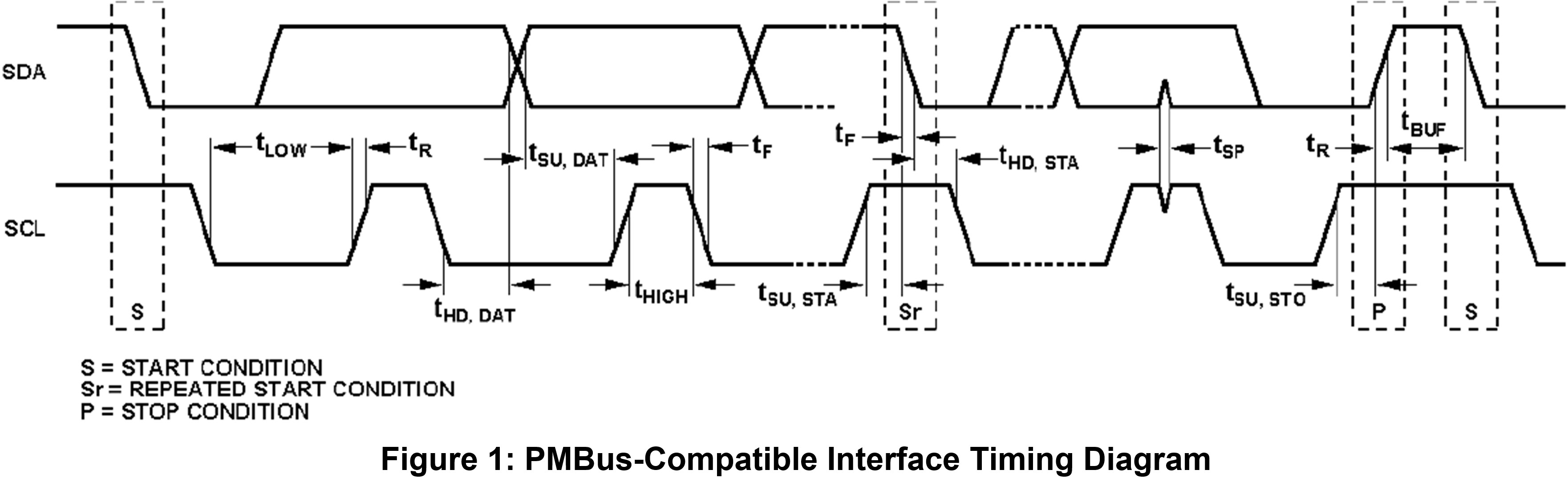
PMBUS PORT SIGNAL CHARACTERISTICS
VIN = 12V, VEN = 2V, TA = -40°C to +125°C, typical values tested at TJ = 25°C, unless otherwise noted.
Parameters
Symbol
Condition
Min
Typ
Max
Units
PMBus Interface Specifications
Input logic low
VIL
0
0.4
V
Input logic high
VIH
1.3
V
Output logic low
VOL
ILOAD = 3mA
0.4
V
SCL clock frequency
fSCL
400
kHz
SCL high time
tHIGH
0.6
μs
SCL low time
tLOW
1.3
μs
Data set-up time
tSU,DAT
100
ns
Data hold time
tHD,DAT
0
0.9
μs
Set-up time for repeated start
tSU,STA
0.6
μs
Hold time for start
tHD,STA
0.6
μs
Bus free time between a start and a stop condition
tBUF
1.3
μs
Set-up time for stop condition
tSU,STO
0.6
μs
Rise time of SCL and SDA
tR
20 + 0.1 × CB
120
ns
Fall time of SCL and SDA
tF
20 + 0.1 × CB
120
ns
Pulse width of suppressed spike
tSP
0
50
ns
Capacitance bus for each bus line
CB
400
pF
TYPICAL PERFORMANCE CHARACTERISTICS
All waveforms simuated.
EFFICIENCY
VIN = , VOUT = , IOUT =
LINE TRANSIENT
Vlow = , Vhigh = , Iout = , Slew rate =
START-UP
VIN = , IOUT =
VIN SHUTDOWN
VIN = , IOUT =
STEADY STATE RIPPLE
VIN = , IOUT =
LOAD TRANSIENT
VIN = , IHIGH = , ILOW = , Slew Rate =
SCP
VIN =
BODE PLOT
Bandwith = , Phase Margin = , Gain Margin =
FUNCTIONAL BLOCK DIAGRAM
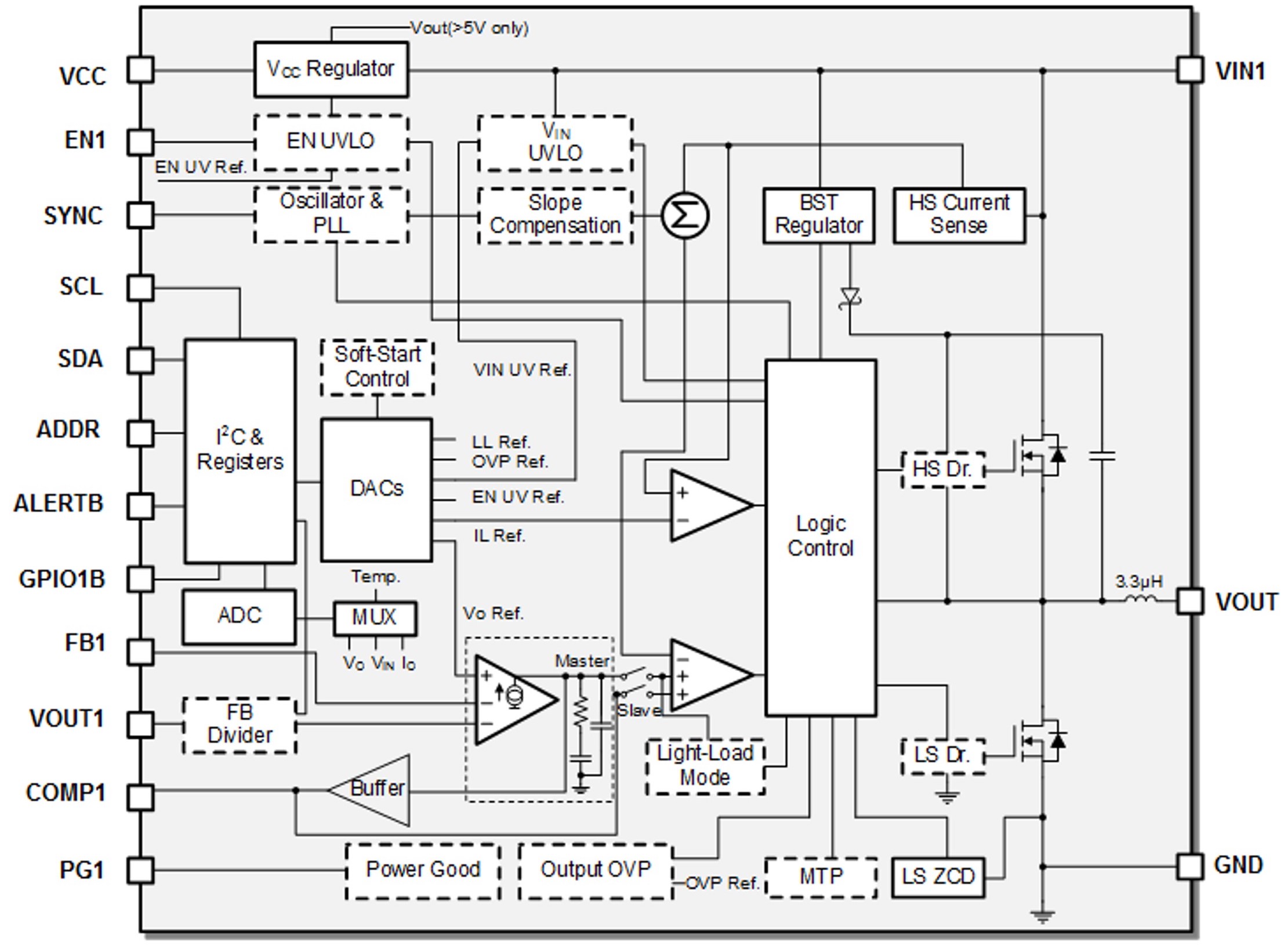
Figure 2: Functional Block Diagram
(Only one channel is shown, blocks in dashed line are programmable via the PMBus)
OPERATION
This device is a high-frequency, synchronous, step-down converter with built-in power MOSFETs. Figure 2 shows a block diagram of the part. It is available with a wide 3.3V to 45V input supply range, and can achieve up to 3A continuous output current per phase, or parallel for 6A total output current. It can also be paralleled for 4-phase and 6-phase operation. The device offers excellent load and line regulation over an ambient temperature range of -40°C to +125°C.
PWM Control
At moderate to high output current, the device operates in a fixed-frequency, peak current control mode to regulate the output voltage. An internal clock initiates a pulse-width modulation (PWM) cycle. At the rising edge of the clock, the high-side switch (HS-FET) turns on, and the inductor current rises linearly to provide energy to the load. The HS-FET remains on until its current reaches the COMP voltage, which is the output of the internal error amplifier. The output voltage of error amplifier depends on the difference of output feedback voltage and the internal high-precision reference, which decides how much energy should be transferred to the load. The higher the load current, the higher the COMP voltage will be. Both the feedback divider ratio and reference can be adjusted by the PMBus, which makes it easy to adjust for different output voltages.
When the HS-FET is off, the low-side switch (LS-FET) turns on immediately and remains on until the next clock cycle starts. During this time, the inductor current flows through the LS-FET. In order to avoid shoot-through, dead time so the HS-FET and LS-FET are not turned on at the same time.
If the current in the HS-FET does not reach COMP set current value in one PWM period, the HS-FET remains on, saving a turn-off operation.
Mode Selection (AAM and Forced CCM)
This device can work in light-load AAM or forced CCM mode, determined by the PMBus. AAM (advanced asynchronous modulation) mode is employed to optimize the efficiency during light-load or no-load conditions. Forced CCM can maintain a constant switching frequency and smaller output ripple, but has low efficiency at light load.
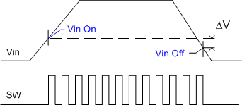
If AAM mode is enabled with load decreasing, the device first enters discontinuous conduction operation (DCM) and maintains a fixed frequency as long as the inductor current approaches zero. If the load is further decreased, or there is no load that makes the inductor peak current lower than the AAM peak current threshold set by the PMBus, the device enters sleep mode and consumes low quiescent current to further improve light-load efficiency. In sleep mode, the internal clock is blocked, and the device skips some pulses. Then the feedback voltage is below the reference, so VCOMP ramps up until the inductor peak current exceeds the AAM threshold. The internal clock resets, and the crossover time is taken as the benchmark of the next clock cycle. This control scheme helps achieve high efficiency by scaling down the frequency to reduce switching and gate driver losses (see Figure 3).
As the output current increases from a light-load condition, VCOMP and the switching frequency increase. If the output current exceeds the critical level set by VCOMP, the device resumes fixed-frequency PWM control.
When forced CCM is enabled, the device operates in a fixed-frequency peak current control mode to regulate the output voltage, regardless of the output current.
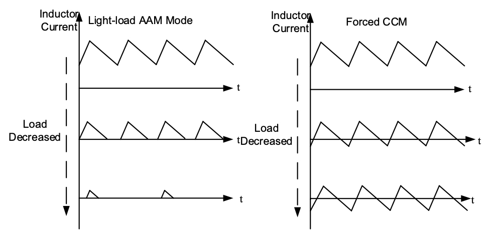
Figure 3: AAM and Forced CCM
Internal Regulator
A 5V internal regulator powers most of the internal circuitries. This regulator takes VIN and operates in the full VIN range. When VIN exceeds 5.0V, the output of the regulator is in full regulation. Lower VIN values result in lower output voltages. The regulator is enabled when VIN exceeds its UVLO threshold and EN is high. In EN shutdown mode, the internal VCC regulator is disabled to reduce power dissipation.
For better thermal performance, BIAS mode can be selected by the PMBus. If VOUT is above 5V, VCC and the internal circuit are powered by VOUT.
Enable Control
EN is a digital control pin that turns the regulator, including the PMBus block, on and off. Drive EN high to turn on the regulator; drive it low to turn the regulator off. The EN threshold can be programmed by the PMBus. An internal 5MΩ resistor from EN to GND allows EN to be floated to shut down the chip.
Oscillator Frequency
The default frequency of this device is 500kHz, and it can be programmed from 300kHz to 2.5MHz by the PMBus. The frequency can also be set by a logic-level synchronous signal.
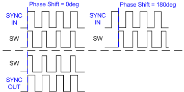
SYNC IN and SYNC OUT
The SYNC pin can be programmed by the PMBus to SYNC IN or SYNC OUT. When operating as SYNC IN, the internal oscillator frequency can be synchronized by an external clock via this pin. At start-up, the device first operates at the internal set frequency, and quickly synchronizes to the external clock once soft start is ready. Ensure the high amplitude of the SYNC clock is above 1.8V and the low amplitude is below 0.4V to drive the internal logic. The recommended external SYNC frequency range is 250kHz to 2.2MHz.
The device operates in forced CCM mode with fixed frequency when there is a SYNC clock, regardless of output current. A pulse longer than 200ns is recommended in application.
When the SYNC pin is set to SYNC OUT, the device outputs the internal clock with a 0° or 180° phase shift. With this function, two devices can operate in same frequency, but 180° out of phase, to reduce the total input current ripple so a smaller input bypass capacitor can be used.
Under-Voltage Lockout (UVLO)
The device has input under-voltage lockout protection (UVLO) to ensure reliable output power. If EN is active, the device is powered on when the input voltage exceeds the UVLO rising threshold, and is powered off when the input voltage drops below the UVLO falling threshold. The UVLO threshold can be set between 3.3V and 5.7V by the PMBus. This function prevents the device from operating at an insufficient voltage. It is a non-latch protection.
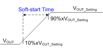
Soft-Start
The device has built-in soft start (SS), which ramps up the output voltage at a controlled slew rate when EN goes high, avoiding overshoot during start-up. When the chip starts, the internal circuitry generates a soft-start voltage that ramps up slowly. When the SS voltage (VSS) is below the internal reference (VREF), VSS overrides VREF as the error amplifier reference. When VSS exceeds VREF, VREF acts as the reference. At this point, soft start finishes and the device enters steady-state operation.
The SS time is internally set to 1ms as a default, and can also be set to 0.5ms, 2ms, or 4ms by the PMBus. When the output voltage shorts to GND, the feedback voltage is pulled low, and VSS is discharged. The part soft starts again when it returns to normal conditions.
Pre-Bias Start-Up
For this device, at start-up, if the output feedback voltage is greater than VSS (which means output has pre-bias voltage), neither the HS-FET or LS-FET turn on until VSS exceeds the feedback voltage.
Power Good Indicator
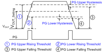
The device has power good (PG) indication. The PG pin is the open drain of a MOSFET. It should be connected to a voltage source through a resistor (e.g. 100kΩ). In the presence of an input voltage, the MOSFET turns on so that the PG pin is pulled to GND before soft start is ready. When the output voltage is within the default ±10% window of rated voltage, PG is pulled high after a delay (typically 30μs). If VOUT moves outside the default ±10% range with a hysteresis, the device pulls PG low to indicate a failure output status. Both the PG threshold and hysteresis can be programmed by the PMBus.
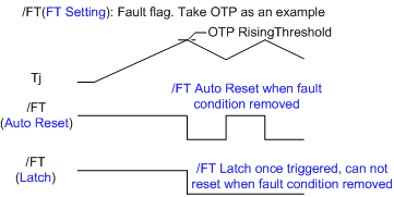
FAULT Indicator
The /FT pin is also an open drain of a MOSFET. It should be connected to a voltage source through a resistor (e.g. 100kΩ). /FT is pulled high in normal operation, and any fault or warning pulls this pin low to indicate a fault status, including input OVP, output OVP, SCP, and thermal shutdown.
Over-Current Protection (OCP)
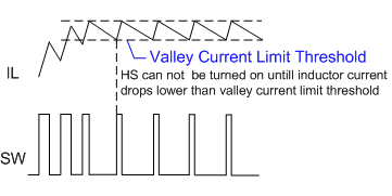
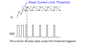
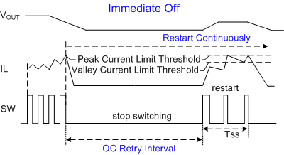
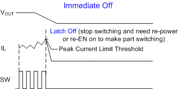
The device has cycle-by-cycle, over-current limit control. The inductor current is monitored during the HS-FET on state. Once the inductor peak current exceeds the set current limit threshold, the HS-FET immediately turns off. Then the LS-FET turns on to discharge the energy, and the inductor current decreases. The HS-FET does not turn on again until the inductor current falls below the valley current limit. This function helps prevent the inductor current from running away and possibly damaging the components. Both the peak current and valley current threshold can be programmed by the PMBus.
When the peak current limit is triggered, the OCP timer starts immediately. The OCP timer can be set to 32, 64, 128, or 256 cycles by the PMBus. Reaching the current limit in each cycle of this OCP timer triggers SCP operation (hiccup as default), which is detailed in the following section.
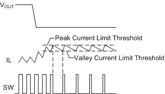
Short-Circuit Protection (SCP)
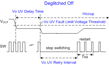
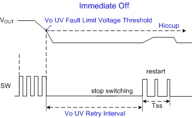
When a short circuit occurs, the device immediately reaches its current limit. Meanwhile, the output voltage quickly drops to the under-voltage threshold (default is 50% of the setting output). The device considers this an output dead short, and directly triggers SCP operation. Three modes can be selected by the PMBus for SCP operation: hiccup as default, switching with non-hiccup, and latch-off.
In default hiccup mode, the device disables its output power stage and resets the soft-start voltage, then initiates a soft start procedure. The off time is determined by the soft-start time and hiccup duty, which can both be set by the PMBus. If the short-circuit condition remains after soft start ends, the device repeats this operation until the short circuit disappears and the output returns to the regulation level. This protection mode greatly reduces the average short-circuit current by periodically restarting the part to alleviate thermal issues and protect the regulator.
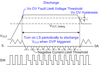
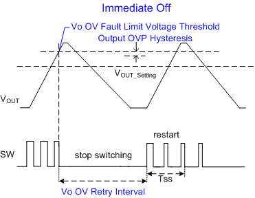
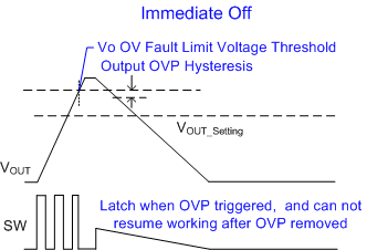
Over-Voltage Protection (OVP)
The device monitors the output voltage through the VOUT pin to detect output over-voltage conditions. When the output voltage exceeds the OVP threshold (default is 120% of the setting voltage), OVP mode is triggered. Three modes can be selected by the PMBus for OVP operation: disable as default, discharge, and latch-off.
The device also has optional input OVP. The threshold can be set to 28V or 34V. If VIN exceeds this threshold, the device stops switching. This is a non-latch protection; the device resumes normal operation once the input OVP is removed.
Thermal Shutdown
The device employs thermal protection by internally monitoring the IC temperature. This function prevents the chip from operating at exceedingly high temperatures. If the junction temperature exceeds the threshold (default 175°C), it shuts down the whole chip. This is a non-latch protection, and there is a default 25°C hysteresis. Once the junction temperature drops to about 150°C, the device resumes normal operation by initiating a soft start. Both the OTP threshold and hysteresis can be set by the PMBus.
Floating Driver and Bootstrap Charging
An internal, built-in bootstrap capacitor powers the floating HS-FET driver. When the voltage difference between BST and SW is less than the internal 5V bootstrap regulator, a PMOS pass transistor M1 connected from VIN to BST turns on to charge the bootstrap capacitor. The current path is through D1, M1, C4, L1, and C2 (see Figure 4). If VIN - VSW exceeds 5V, U1 will regulate M1 to maintain a 5V BST voltage across C4. Meanwhile, the external circuit must have enough voltage headroom to accommodate charging. A 10Ω resistor placed between SW and the BST capacitor is strongly recommended to reduce SW spike voltage.
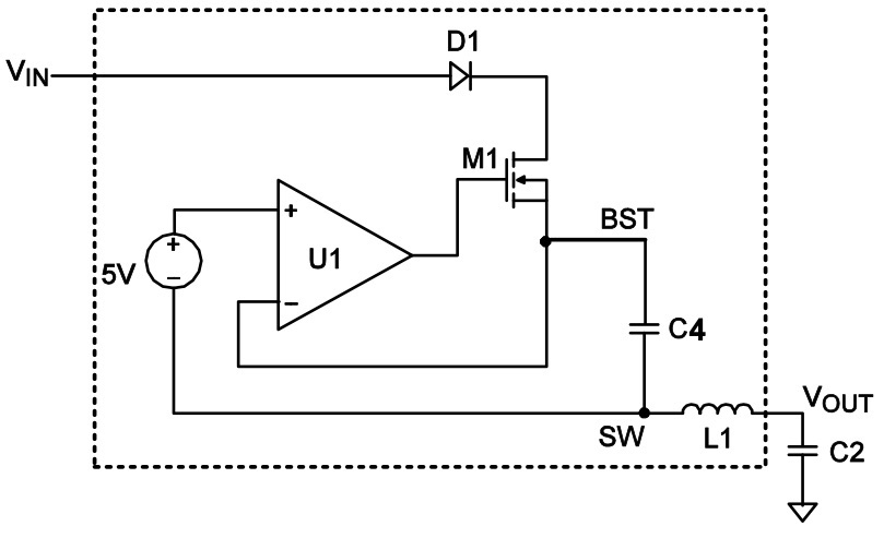
Figure 4: Internal Bootstrap Charging Circuit
As long as VIN is sufficiently higher than VSW, the bootstrap capacitor can be charged. When the HS-FET is on, VIN is about equal to VSW so the bootstrap capacitor cannot charge. The best charging period occurs when the LS-FET is on so that VIN - VSW is at its largest. When there is no current in the inductor, VSW equals VOUT, so the difference between VIN and VOUT can charge the bootstrap capacitor.
In higher duty cycle operation conditions, the internal charging circuit may not have sufficient voltage and time to charge the bootstrap capacitor. In this case, extra external circuitry can be used to ensure the bootstrap voltage is in the normal operation range.
Low-Dropout Operation (BST Refresh)
To improve dropout, the device is designed to operate at close to 100% duty cycle as long as the BST-to-SW voltage is greater than 2.5V. When the voltage from BST to SW drops below 2.5V, the HS-FET turns off using a UVLO circuit, which allows the LS-FET to conduct and refresh the charge on the BST capacitor.
In cases where the input voltage drops, the HS-FET remains on and close to 100% duty cycle to maintain output regulation, until the BST-to-SW voltage falls below 2.5V. Since the supply current sourced from the BST capacitor is low, the HS-FET can remain on for more switching cycles than are required to refresh the capacitor. Therefore, the effective duty cycle of the switching regulator is high.
The effective duty cycle during dropout of the regulator is mainly influenced by the voltage drops across the power MOSFET, inductor resistance, low-side diode, and PCB resistance.
PMBus Control and Default Output Voltage
When the device is enabled (EN = high and VIN > UVLO), the chip starts up to a default 5V output voltage. After that, the PMBus can communicate with the master. Once the PMBus receives valid output voltage set instructions, the output voltage is determined by the PMBus control.
The output voltage setting is set by adjusting the internal reference voltage and output feedback divider ratio. After the device receives a valid data byte of output voltage setting, it searches the corresponding value from the truth table, sends the command of adjusting reference and divider ratio, and finally outputs the right voltage.
CRC Protection
The integrity of OTP is checked after a power-cycle reset. Each time the registers read the OTP contents, the device performs a CRC check. If a CRC error occurs, the registers will try to read two more times. If the error still occurs, the register will read the next available OTP page. If there is no available OTP page, then the CML bit is set in the STATUS_BYTE and STATUS_WORD commands, the appropriate bit is set in the STATUS_MFR_SPECIFIC command, and the ALERTB pin is pulled low.
PMBUS INTERFACE
PMBus Serial Interface Description
PMBus is a two-wire, bidirectional serial interface, consisting of a data line (SDA) and a clock line (SCL). The lines are externally pulled to a bus voltage when they are idle. Connecting to the line, a master device generates the SCL signal and device address, and arranges the communication sequence. The device interface is a PMBus slave that supports both fast mode (400kHz) and high-speed mode (3.4MHz), adding flexibility to the power supply solution. The output voltage, transition slew rate, and other parameters can be instantaneously controlled via the PMBus interface.
Data Validity
One clock pulse is generated for each data bit transferred. The data on the SDA line must be stable during the high period of the clock. The high or low state of the data line can only change when the clock signal on the SCL line is low (see Figure 5).
Figure 5: Bit Transfer on the PMBus
Start and Stop Conditions
The start and stop conditions are signaled by the master device, which signifies the beginning and the end of the PMBus transfer. A start condition (S) is defined as the SDA signal transitioning from high to low while the SCL is high. A stop condition (P) is defined as the SDA signal transitioning from low to high while the SCL is high (see Figure 6).
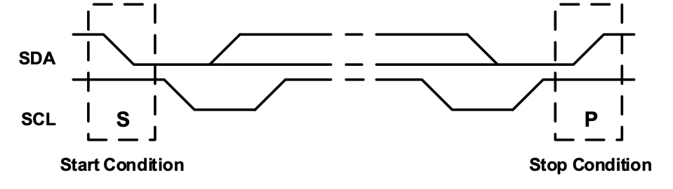
Figure 6: Start and Stop Conditions
Start and stop conditions are generated always by the master. The bus is considered busy after the start condition. The bus is considered free again after a minimum of 4.7µs after the stop condition. The bus stays busy if a repeated start (Sr) is generated instead of a stop condition. The start and repeated start conditions are functionally identical.
Transfer Data
Every byte put on the SDA line must be 8 bits long. Each byte must be followed by an acknowledge (ACK) bit. The acknowledge-related clock pulse is generated by the master. The transmitter releases the SDA line (high) during the acknowledge clock pulse. The receiver must pull down the SDA line during the acknowledge clock pulse, so that it remains stable low during the high period of the clock pulse.
Figure 7 shows the format that data transfers follow. After the start condition, a slave address is sent. This address is 7 bits long followed by an 8th data direction bit (R/W). A 0 indicates a transmission (write), and a 1 indicates a request for data (read). A data transfer is terminated always by a stop condition, generated by the master. However, if a master still wishes to communicate on the bus, it can generate a repeated start condition and address another slave without first generating a stop condition.
Figure 7: A Complete Data Transfer
PMBus Update Sequence
The device requires a start condition, a valid PMBus address, a register address byte, and a data byte for a single data update. After receipt of each byte, the device acknowledges by pulling the SDA line low during the high period of a single clock pulse. A valid PMBus address selects the device. The device performs an update on the falling edge of the LSB byte.
Device PMBus Chip Address
The ADD pin can be used to program the PMBUS address. The device supports seven addresses for up to seven voltage rails through configuring the resistor value that connecting between the ADD pin and ground. When the master sends the address as an 8-bit value, the 7-bit address should be followed by “0/1” to indicate a write/read operation.
Table 1 shows the resistor values for different PMBus addresses.
Table 1: PMBus Address| Resistor (kΩ) 1% | Address |
|---|---|
| 0 | 21h |
| 12.5 + 25 | 22h |
| 12.5 + 50 | 23h |
| 12.5 + 75 | 24h |
| 12.5 + 100 | 25h |
| 12.5 + 125 | 26h |
| 12.5 + 150 | 27h |
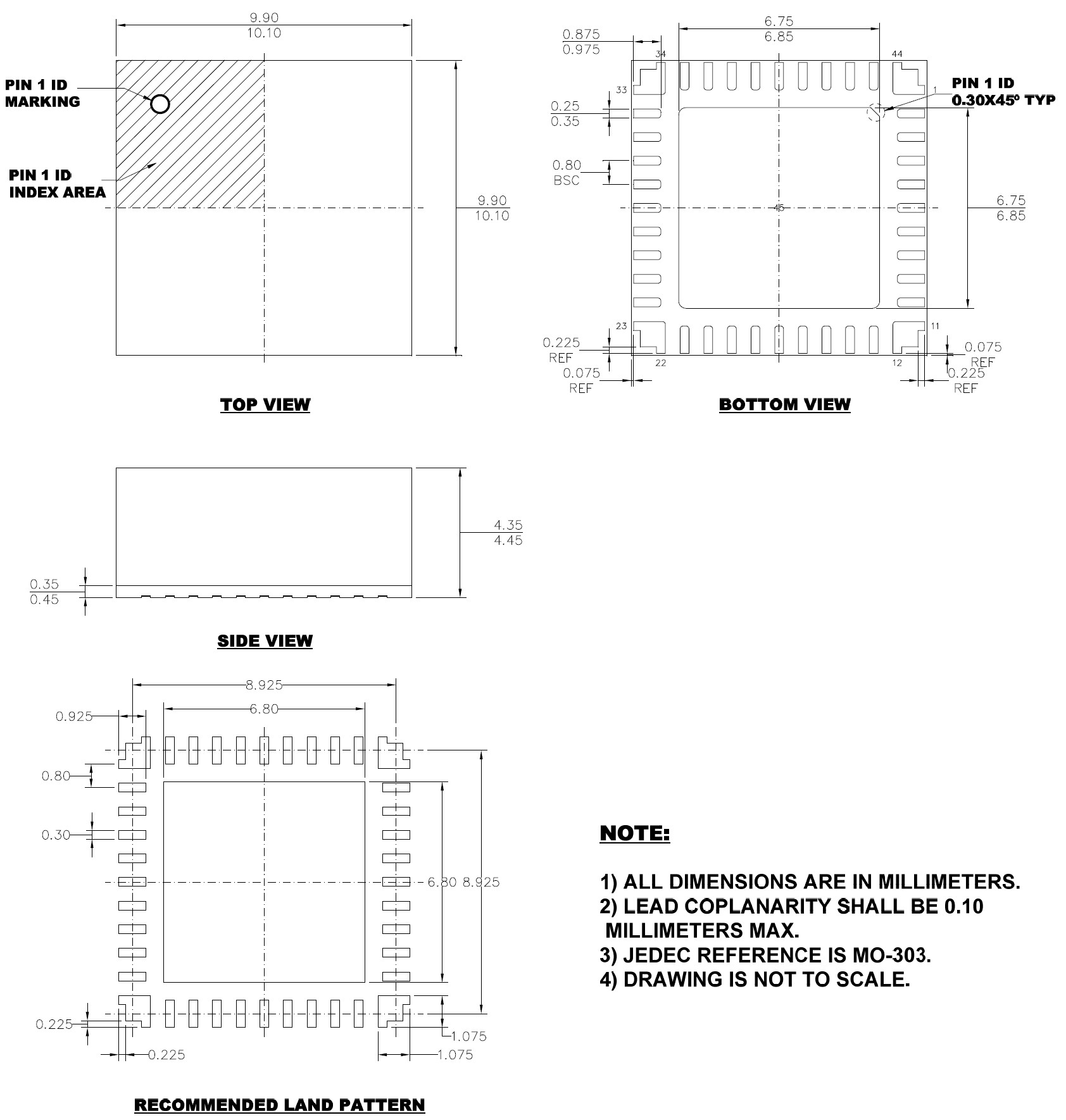
PACKAGE INFORMATION
LGA-45 (10mmx10mmx4.4mm)
NOTICE: The information in this document is subject to change without notice. Please contact MPS for current specifications. Users should warrant and guarantee that third-party Intellectual Property rights are not infringed upon when integrating MPS products into any application. MPS will not assume any legal responsibility for any said applications.
MonolithicPower.com
07-23-2026 - MPS Proprietary Information. Patent Protected. Unauthorized Photocopy and Duplication Prohibited.
Preliminary Specificatios Subject to Design Finalization**
© 2026 MPS. All Rights Reserved.
Sale Price
The mEZDPD4506 series are scalable, programmable DC/DC power supplies with up to 6A peak output current. There are two packages available: the mEZDPD4506AS is a surface mount (LGA package), and the mEZDPD4506A is in a DIP (Dual Inline Package).

Digital programmable features enable the mEZDPD4506AS to be controlled and programmed via an I2C PMBus. Operation parameters can be programmed, including compensation, the output voltage transition slew rate, the switching frequency, and power save mode. Pre-configured DIP package modules are available to provide quick evaluation.
Want your custom configuration pre-loaded to the evaluation board module? Create and save a module configuration and order evaluation board here.
 Learn about our Evaluation Kit
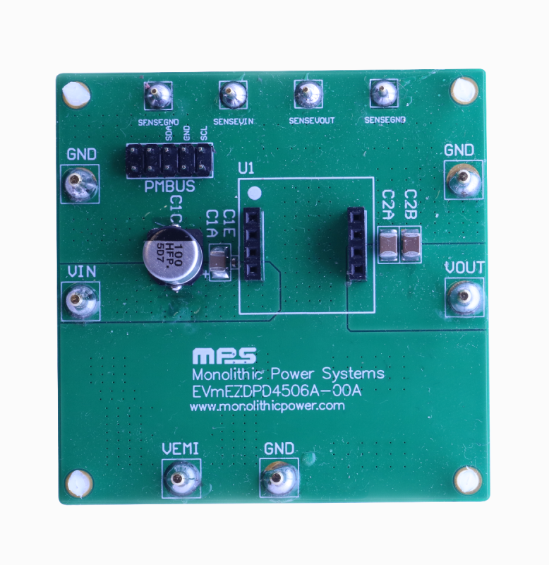
Evaluation board for the mEZDPD4506A configurable power module.
The EVmEZDPD4506A is the evaluation board for the mEZDPD4506A configurable DC/DC power module with up to 6A and 0.6-24V output voltage. This part has a multiple time programmable memory and can be programmed with the Virtual Bench Pro GUI software available below.
Use the GUI to configure and monitor part performance such as Vin, Vout, Iout & Temperature. Current and output voltage values are all that is needed to start evaluation. Additional parameters have default settings and can be re-configured as needed.
$25.00 + tax

Evaluation kit for the mEZDPD4506A configurable power module.
The PKT-mEZDPD4506A is the evaluation kit for the mEZDPD4506A configurable DC/DC power module with up to 6A and 0.6-24V output voltage. This part has a multiple time programmable memory and can be programmed with the Virtual Bench Pro GUI software available below.
Use the GUI to configure and monitor part performance such as Vin, Vout, Iout & Temperature. Current and output voltage values are all that is needed to start evaluation. Additional parameters have default settings and can be re-configured as needed.
$95.00 + tax
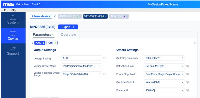
Graphical User Interface (GUI) Supported by MPS Used to Configure and Monitor Multiple MPS Digital Power Solutions with an I2C Interface
The Virtual Bench Pro 4.0 is a Graphical User Interface (GUI) supported by MPS used to configure and monitor multiple MPS digital power solutions with an I2C Interface. This GUI is an intuitive tool that can be used with MPS evaluation kits and helps assist in the evaluation and testing phases of your design.
Hardware & Software Requirements:
- USB to I2C Communication Device EVKT-USBI2C-02
- PC running Window 10 or later
- .Net Framework 4.0 or later
- RAM: 2GB of free RAM
- CPU: Any modern CPU
- Disk Space: 2GB
- Monitor Resolution: 1024x768
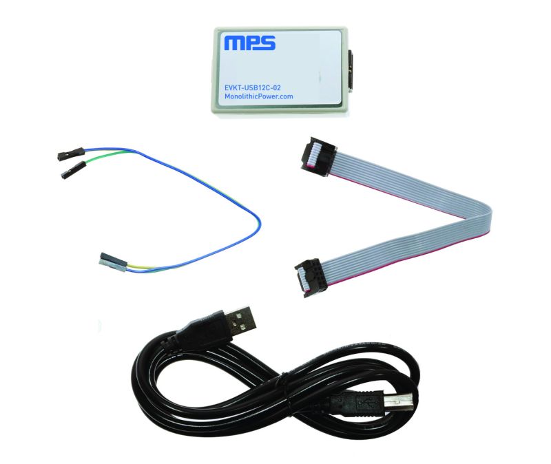
Communication Interface Device USB to I2C/PMBus, included with product evaluation kit or can be purchased separately.
The EVKT-USBI2C-02 is included with product evaluation kits, or it can be purchased separately. EVKT-USBI2C-02 provides the communication interface for USB to I2C or USB to PMBus. It is designed to work with MPS I2C and PMBus products, and Virtual Bench Pro, and I2C GUI tools. USB driver will install automatically or download directly.
The EVKT-USBI2C-02 kit includes:
- 1 USB to I2C communication device interface
- 1 USB cable
- 1 10-pin ribbon cable
- 1 3-pin ribbon cable
- Datasheet and driver files
$50.00 + tax

Technical Forum
Questions answered by MPS engineers in 24h
mEZDPD4506AS change settings without a development board
Hello. Purchase mEZDPD4506AS and leave an inquiry while using it. I want to change the UVP and OVP Mode of mEZDPD4506AS to 'Igno...
DC-DC POWER CONVERTERS
 Latest activity 4 years ago
 3 Comments
mEZDPD4506AS pin out sip
...chnical drawing with all the distance measurements of the Configurable DC/DC Step-Down Power Module mEZDPD4506AS in the DIP housing version? Can an...
INTEGRATED INDUCTOR POWER MODULES
Latest activity 5 years ago
3 Comments
mEZDPD4506AS Circuit Review
hello. I am curious about the mEZDPD4506AS product. I would like to combine 2 channels into one channel and output 12V to 7V@6A. I plan to pro...
DC-DC POWER CONVERTERS
Latest activity a year ago
5 Comments
Quality Policy, Certificates & Reliability Reports
All MPS parts are lead-free, halogen-free and adhere to the RoHS directive. See Environmental section for details.


Log in to your account
Your email must be verified before you can log in. A message with a link to complete the verification process has been sent to your email address.
Create New Account
Forgot Password
Log in to continue
myMPS+
A Plus account is required to perform this action. Log in to your myMPS+ account or create one now.
Don’t have a myMPS+ account yet?
Get early access to new products, datasheets,
and free samples.