mEZDPD1620AS continues to be in production for existing customers. Please consider this alternative for new designs:
MPM3695GPJ-20
MPM3695GPJ-20
3V to 16V Input, Continuous 25A Power Module
Features & Benefits
- Wide Input Voltage (VIN) Range from 3V:
- 3V to 16V VIN with External VCC
- 4V to 16V VIN with Internal VCC
- 0.5V to 5.5V Output Voltage (VOUT) Range
- 25A of Continuous Output Current (IOUT)
- Automatic Interleaving for Multi-Phase Operation
- Automatic Compensation with Adaptive Multi-Phase Constant-On-Time (MCOT) for Ultra-Fast Transient Response
- ±1% Reference Voltage (VREF) Accuracy ( -40°C to +125°C)
- True VOUT Remote Sense
- Pre-Biased Output
- Telemetry Readback Including VIN, VOUT, IOUT, Temperature, and Faults
- Built-In Multiple-Time Programmable (MTP) Memory to Store Custom Configurations
- Configurable via the Digital Interface:
- Current Limit
- Pulse-Skip Mode (PSM) or Continuous Conduction Mode (CCM) Selection
- Soft-Start Time (tSS)
- Switching Frequency (fSW) Selection: 400kHz, 600kHz, 800kHz, or 1000kHz
- Fault Limits
- Ramp Compensation
- Available in an ECLGA-29 (5mmx6mmx4.4mm) Package
… and many more!
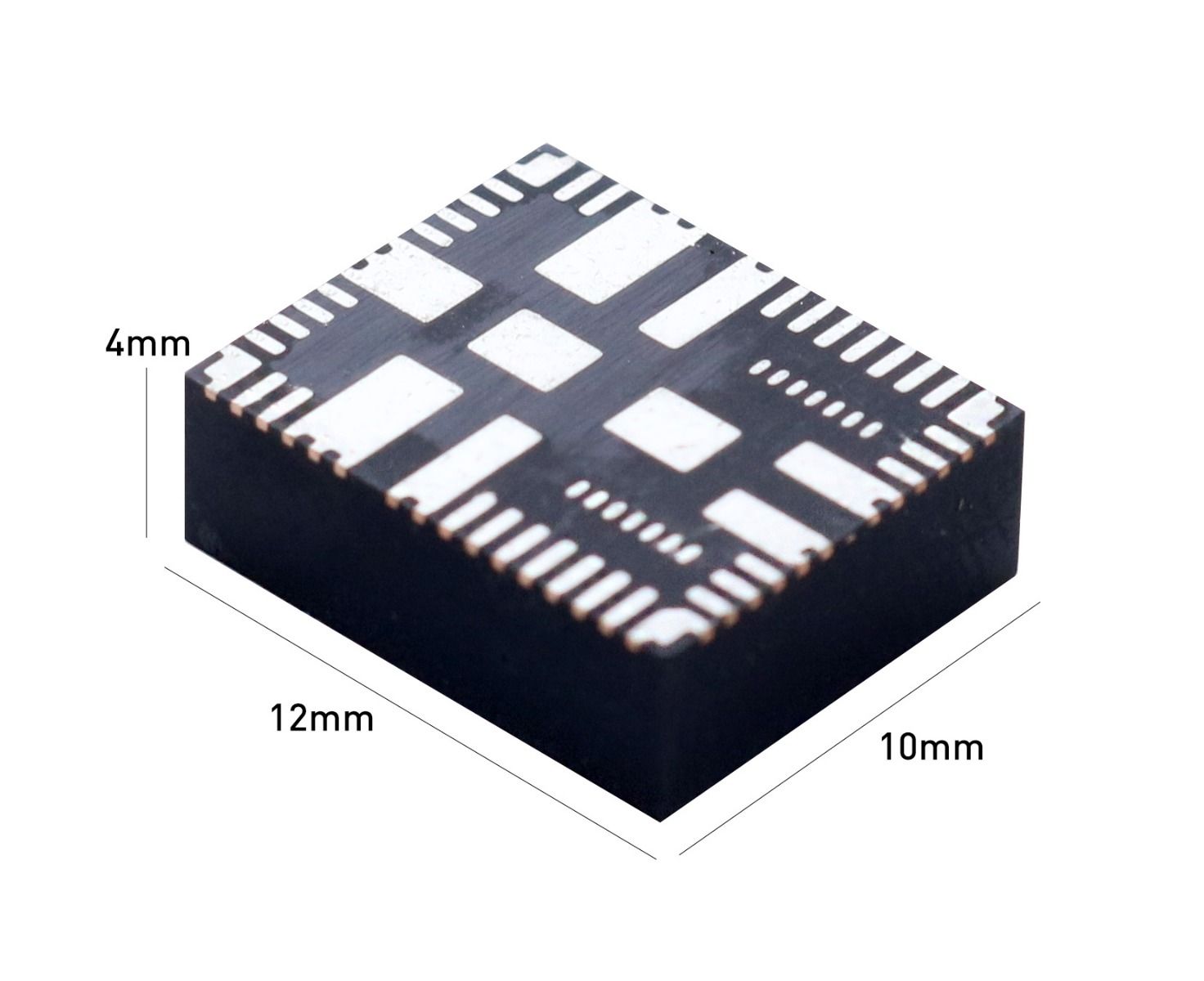
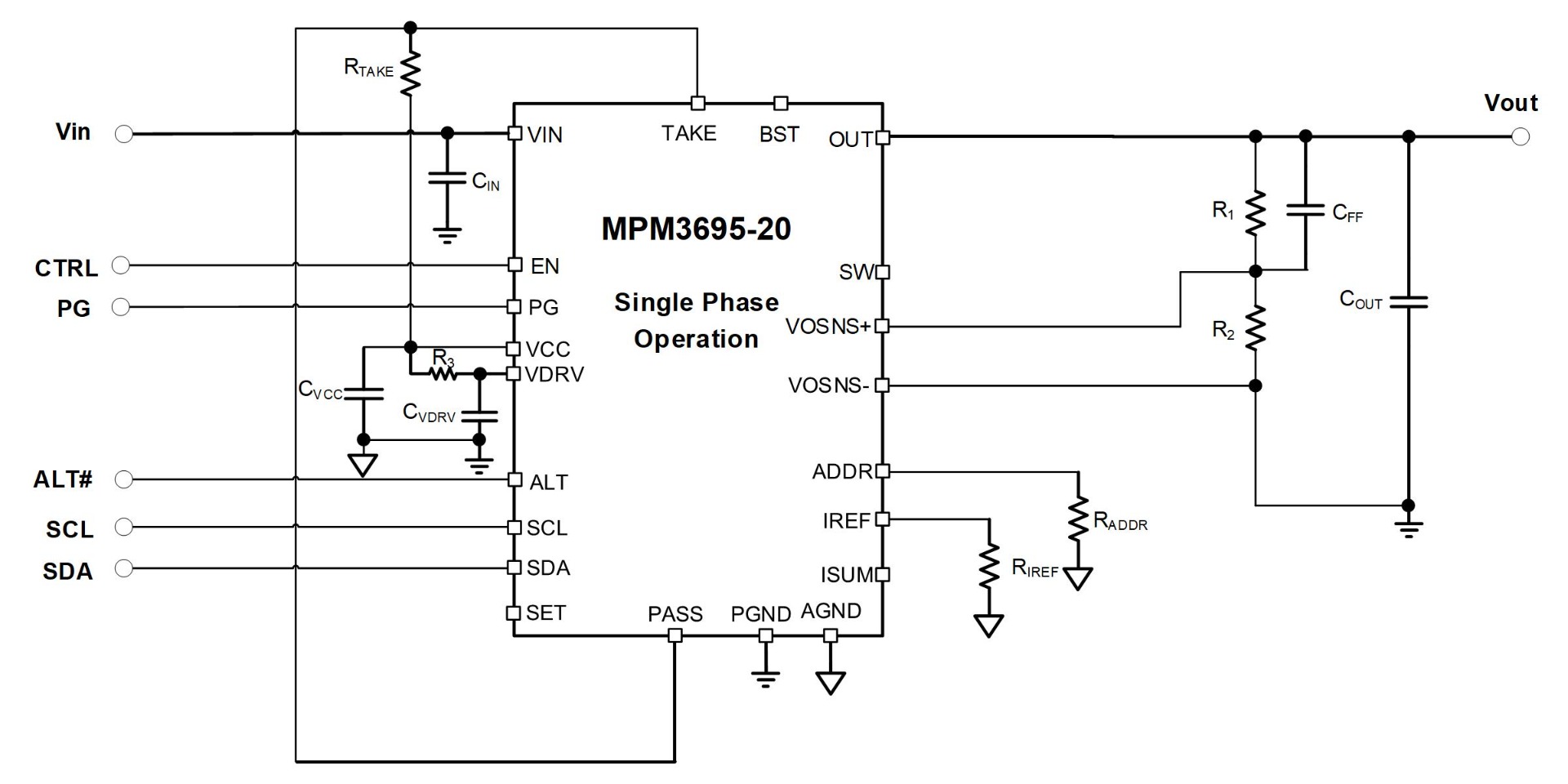
The mEZDPD1620AS is a configurable DC/DC step-down power module up to 25A peak and 16V input voltage. This part has a multiple time programmable memory and a simple GUI to program. Comes in a convenient QFN Package (10mmx12mmx4mm).
Sale Price
The mEZDPD1620 series are scalable, programmable DC/DC power supplies with up to 25A peak output current. There are two packages available: the mEZDPD1620AS is a surface mount (QFN package), and the mEZDPD1620A is in the DIP (Dual Inline Package).

Digital programmable features enable the mEZDPD1620AS to be controlled and programmed via an I2C PMBus. Operation parameters can be programmed, including compensation, the output voltage transition slew rate, the switching frequency, and power save mode. Pre-configured DIP package modules are available to provide quick evaluation.
Want your custom configuration pre-loaded to the evaluation board module? Create and save a module configuration and order evaluation board here
 Learn about our Evaluation Kit
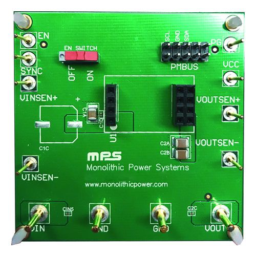
Evaluation board for the mEZDPD1620A configurable power module.
The EVmEZDPD1620A is the evaluation board for the mEZDPD1620A configurable DC/DC power module with up to 20A and 0.6-5.5V output voltage. This part has a multiple time programmable memory and can be programmed with the Virtual Bench Pro GUI software available below.
Use the GUI to configure and monitor part performance such as Vin, Vout, Iout & Temperature. Current and output voltage values are all that is needed to start evaluation. Additional parameters have default settings and can be re-configured as needed.
Want your custom configuration pre-loaded to the eval module? Create and save a module configuration here
$25.00 + tax
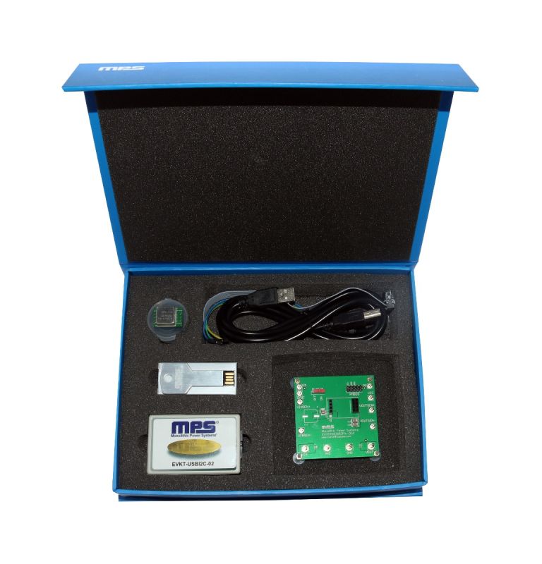
Evaluation kit for the mEZDPD1620A configurable power module.
The PKT-mEZDPD1620A is the evaluation kit for the mEZDPD1620A configurable DC/DC power module with up to 20A and 0.6-5.5V output voltage. This part has a multiple time programmable memory and can be programmed with the Virtual Bench Pro GUI software available below.
Use the GUI to configure and monitor part performance such as Vin, Vout, Iout & Temperature. Current and output voltage values are all that is needed to start evaluation. Additional parameters have default settings and can be re-configured as needed.
Want your custom configuration pre-loaded to the eval module? Create and save a module configuration here
$95.00 + tax
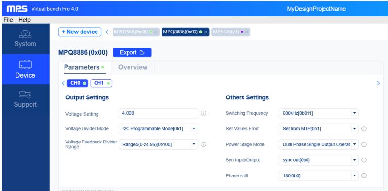
Graphical User Interface (GUI) Supported by MPS Used to Configure and Monitor Multiple MPS Digital Power Solutions with an I2C Interface
The Virtual Bench Pro 4.0 is a Graphical User Interface (GUI) supported by MPS used to configure and monitor multiple MPS digital power solutions with an I2C Interface. This GUI is an intuitive tool that can be used with MPS evaluation kits and helps assist in the evaluation and testing phases of your design.
Hardware & Software Requirements:
- USB to I2C Communication Device EVKT-USBI2C-02
- PC running Window 10 or later
- .Net Framework 4.0 or later
- RAM: 2GB of free RAM
- CPU: Any modern CPU
- Disk Space: 2GB
- Monitor Resolution: 1024x768
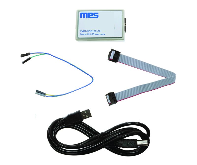
Communication Interface Device USB to I2C/PMBus, included with product evaluation kit or can be purchased separately.
The EVKT-USBI2C-02 is included with product evaluation kits, or it can be purchased separately. EVKT-USBI2C-02 provides the communication interface for USB to I2C or USB to PMBus. It is designed to work with MPS I2C and PMBus products, and Virtual Bench Pro, and I2C GUI tools. USB driver will install automatically or download directly.
The EVKT-USBI2C-02 kit includes:
- 1 USB to I2C communication device interface
- 1 USB cable
- 1 10-pin ribbon cable
- 1 3-pin ribbon cable
- Datasheet and driver files
$50.00 + tax


Log in to your account
Create New Account