AN178 - MCS180x Family Current Sensor Transient Behavior while Exceeding Current Ratings

Get valuable resources straight to your inbox - sent out once per month
We value your privacy
ABSTRACT
This application note presents the MCS180x family of current sensors’ transient behavior, and the MCS180x’s ability to respond to current spikes (e.g. shorts in the primary circuit).
Applicable Products
| Part Number | Package |
| MCS1800 | SOIC-8 |
| MCS1801 | SOIC-8 |
| MCS1802 | SOIC-8 |
| MCS1803 | SOIC-8 |
| MCS1805 | SOIC-8 |
| MCS1806 | SOIC-8 |
INTRODUCTION
The MCS180x family of sensors are designed to measure current between ±5A and ±50A. The primary current flows through the copper lead frame and generates a magnetic field in the Hall-effect probes integrated into a silicon die. The secondary circuit is isolated galvanically from the primary circuit (see Figure 1). The current sensor includes an output signal proportional to the primary current.
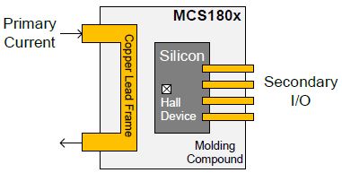
Figure 1: MCS180x Current Sensor
The device can tolerate a certain amount of current above its rated value. However, even if the primary conductor resistance is small (about 1mΩ), heat can dissipate, which may cause the device to fail. Different failure conditions can occur, and are dependent on the amount of current flowing through the primary circuit.
FAILURE CONDITIONS
The primary conductor’s resistance (RT) increases linearly as the temperature (T) increases. RT can be calculated with Equation (1):
$${R_T \over R_{25}} = 1 + α (T - 25ºC) $$Where R25 is the resistance at ambient temperature, and α is 2.8 x 10⁻³ 1/°C. This means that a constant current (CC) dissipates heat with positive feedback. If this heat cannot be sufficiently dissipated, thermal runaway may occur. This shortens the time before a failure occurs as a function of the primary current.
If the temperature exceeds the copper lead frame’s melting point, then the primary circuit conductor may melt and create an open circuit. The heat produced in the lead frame also diffuses across the molding compound inside the package and into the silicon die. The copper lead frame, the mold compound, and the silicon die have different degradation temperatures:
- Lead frame (primary conductor) melting point: 1060°C
- Mold compound point of irreversible degradation: about 260°C to 300°C
- Silicon die absolute maximum temperature: 165°C
The failure is dependent on which of the three degradation temperatures is reached first. The MCS180x family’s current sensor thermal behavior has been studied both numerically and experimentally on the SOIC-8 package.
MEASUREMENTS AND SIMULATION CONDITIONS
In both the numerical and experimental set-up, the MCS180x is mounted onto an evaluation board (1) (see Figure 2 on page 4). The pins are connected electrically and thermally to the board pads via solder bumps.
Note:
1) For more information, refer to the MCS180x datasheets, available on the MPS website.
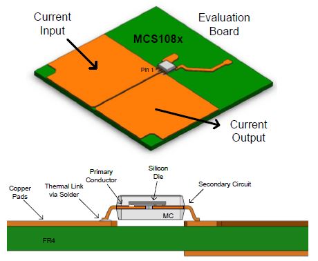
Figure 2: Numerical System Used for Time-Dependent Finite Element Simulations
The whole system is initially at room temperature, and a CC runs to the copper pads. The primary conductor’s resistance (RT) depends on the temperature (T) (see Equation (1) on page 3). The electrical response and thermal response of the applied current are calculated by finite element methods.
RESULTS
Figure 3 shows the summarized results of the simulations.
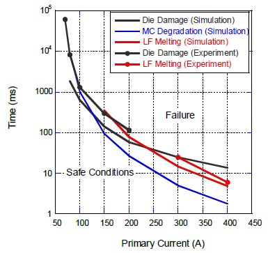
Figure 3: MCS180x Safe Conditions and Failure Conditions Once the Rated Current Has Been Exceeded
Currents above 250A
The lead frame temperature increases rapidly at high currents. For example, at 350A, the copper lead frame reaches its melting point in 10ms. Since the primary conductor creates an open circuit once it melts, the lead frame destruction point can be determined with simulations and experiments. However, simulations show that the molding compound (the thin layer between the lead frame and the die) reaches its damage point before the lead frame reaches its melting point. Even if there is not a short between the primary circuit and the secondary circuit, the characteristics of the isolation layer can be irreversibly altered. To reliably operate the current sensor, the MCS180x must remain in the safe conditions range (see Figure 3 on page 4).
Currents between 150A and 250A
For currents between 150A and 250A, the time before a failure occurs ranges between 10ms and 200ms. The failure mechanism can also be triggered by the molding compound area close to the primary conductor as it reaches its damage temperature. Therefore, the material filling the gap between the primary conductor and the die may also be damaged, resulting in a reduction of primary-to-secondary isolation.
The detailed temperature distribution simulations inside the copper lead frame show that after 25ms, the heat diffuses significantly along the primary conductor via the pin to the PCB. Therefore, anything that occurs after 25ms depends on the MCS180x’s thermal coupling with the PCB. For currents below 200A, since failure occurs after 25ms, the failure conditions depend on the IC’s thermal coupling to the PCB.
Currents between 50A and 150A
For currents between 50A and 150A, the thermal response progresses until the temperature is the same across the device, achieving thermal equilibrium within the package. This means that the silicon die is the critical failure mechanism, as its absolute maximum temperature rating (165°C) can be exceeded before the degradation of the other package components. At 165°C, isolation has not been altered yet, but the sensor characteristics may permanently deviate from datasheet specifications.
CONCLUSION
Currents exceeding the device rating can be applied, but the duration must be limited to values inside the safe area of the current-time plane so that every component of the sensor, including the isolation, remains unaltered (see Figure 3 on page 5).
Above 25ms and up to 10s, the detailed failure mechanism depends on the thermal coupling between the surface-mount component and the PCB. As long as the PCB extends well beyond the SOIC-8 package area, its exact shape does not play a major role. Therefore, regardless of the PCB’s detailed geometry, if the sensor is correctly soldered, the safe condition region is close to the one shown in Figure 3 on page 5. (2)
The key parameters during this transient period is dissipation. Consequently, if a sensor can be exposed to conditions outside of the safe range (see Figure 3 on page 5), then a part with smaller primary conductor resistance must be considered.
Note:
2) For currents above 50A, the PCB shape and the thermal link environment can affect the long-term temperature the device reaches under a DC current.
_______________________
Did you find this interesting? Get valuable resources straight to your inbox - sent out once per month!
Technical Forum
 Latest activity a day ago
 2 Comments
Latest activity a week ago
2 Comments
Latest activity a week ago
2 Comments
2 Comments
Latest activity a week ago
2 Comments
Latest activity a week ago
2 Comments
Log in to your account
Create New Account