Using Filter Capacitors and Inductors to Suppress Radiated EMI

Get valuable resources straight to your inbox - sent out once per month
We value your privacy
Introduction
One of the most common methods to suppress electromagnetic interference (EMI) is to use filter capacitors and inductors. This article explores how to manage radiated EMI by discussing the impedance characteristics and design methodology of these filtering components in a dual active bridge converter.
Radiated EMI Model of a Dual Active Bridge Converter
When the switch tube (M1) turns on within one switching cycle, the current path occurs in the following order: input voltage (VIN), inductance (L), and M1. The inductor current (IL) rises, resulting in energy storage in the inductor (see Figure 1).
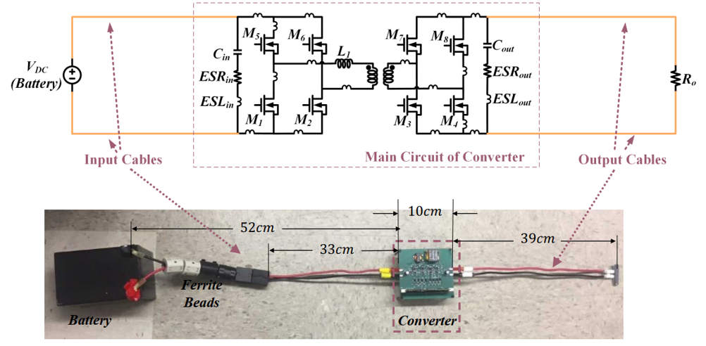
Figure 1: Topology and Physical Diagram of a Dual Active Bridge Converter
Figure 2 shows radiated EMI principles, with Figure 2a on the left showing the dipole antenna’s radiation principles, and Figure 2b on the right showing the general radiated EMI model.
Figure 2a shows that the antenna’s energy flows into three different parts. One part is resonated between the two poles and does not radiate into space, where jXA is the impedance corresponding to the reactive power. The second part of the power is radiated into space, which is modelled with Rr. The last part of the energy is dissipated on the antenna’s resistance, which is modelled with Rl.
Figure 2b shows a general radiated EMI model. The converter can be modeled by an equivalent noise source (VS) and source impedance (represented by the real part, RS, and imaginary part, XS).

Figure 2: Radiated EMI Principles
The CM current (IA) amplitude (|IA|) can be calculated with Equation (1):

Where RA is the sum of Rl and Rr, and the current coefficient (KI) is a coefficient that is proportional to IA.
To determine the radiated EMI, the electromagnetic field intensity generated by the converter at a set distance is measured. Consider the electric field where the maximum value of the electric field intensity (EMAX) at the converter’s distance (r) can be estimated with Equation (2):

Where η is the wave impedance, and D is the directionality. The radius (r) is the ratio of the maximum power density in that direction (D) compared to the average power density of a sphere, and the electric field intensity coefficient (KE) is a coefficient that is directly proportional to the radiated electric field intensity.
The impedances of the antenna and the converter can be obtained through testing. For more information, refer to Part I, Part II, and Part III of our Measuring High-Frequency, CM Current, Voltage, and Impedance article series.
Related Content
-
VIDEO

MPS Isolation Solutions in High-Power and Electrification Systems Enable a Greener Future
Learn how our high power density solutions enhance solar energy, energy storage, and EV systems, ensuring electrical isolation for safety in high-power systems.
-
ARTICLE

Measuring High-Frequency, Common-Mode Current, Voltage, and Impedance (Part I)
This article is the first part of a three-part series discussing measurement methods for high-frequency, common-mode (CM) current, voltage, and impedance using a flyback converter.
-
USE CASE
Isolated Gate Drivers Use Case: Portable Power Stations
This use case considers the application of isolated gate drivers in portable power stations with MPS’s MP188xx family, MP9928, MP4247, and MP5031.
-
ARTICLE

DC Fast Charging System: Maximizing Power Density with an LLC Transformer Driver
Find out how the MPQ18913 simplifies LLC power supplies for high-power charging applications with features including automatic resonant frequency detection and integrated transistors.
Causes of Radiated EMI Spikes
KI can be calculated with Equation (3):

KE can be calculated with Equation (4):

Since XS and XA may be both capacitive and inductive, they can cancel each other out. If the sum of RS and RA is small, a peak is observed on the spectrum.
Figure 3 shows the measurement results of the dual active bridge converter’s source impedance and antenna impedance. The XS and XA curves intersect four times. XS and XA can cancel out each other only when they are in opposite phases (at positions 1 and 2 in Figure 3). Additionally, as RA at position 2 is very large (nearly 1000Ω), it is unlikely that a resonance spike occurs at this point. In contrast, RA at position 1 is only about 100Ω (the frequency at position 1 is approximately 167MHz).
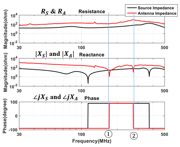
Figure 3: Source Impedance and Antenna Impedance of Dual Active Bridge Converter
Figure 4 shows the KI and KE curves.
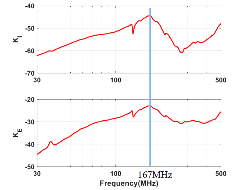
Figure 4: KI and KE Calculations
Figure 5 shows the spectrum of the measured IA and the radiated EMI.
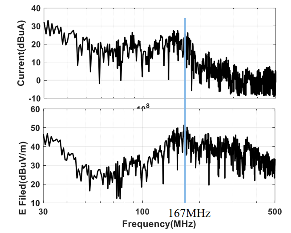
Figure 5: Measured CM Current and Radiated EMI Spectrum
At 167MHz, a resonance spike is observed due to XS and XA canceling out each other, and RS + RA is small. The experimental results can also verify these results.
Impact and Design Methodology of the CM Inductor on Radiated EMI
Adding a CM inductor at the input or output terminals is a popular method to suppress radiated EMI. The inductor’s high-frequency model must typically consider the influence of its equivalent capacitance (CP) and equivalent resistance (RP) (see Figure 6).
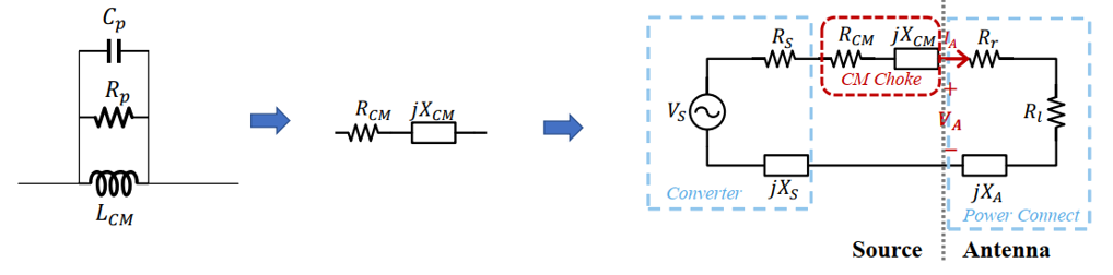
Figure 6: CM Inductance and Radiation Model Considering Inductance
To simplify the radiation model, the inductor model can be expressed as a series form of resistance (RCM) and reactance (XCM). By applying the inductor model to the model shown in Figure 2b, we can obtain the CM inductance and radiation model in Figure 6. It should be noted that both RCM and XCM change with frequency. In this case, KI and KE from Equation (3) and (4) must be modified to calculate for the CM current coefficient (KI_CM) and CM electric field intensity coefficient (KE_CM).
KI_CM can be calculated with Equation (5):

KE_CM can be calculated with Equation (6):

The CM inductor has three effects on radiation:
- The resonance frequency in the radiated EMI spectrum shifts.
- The resistance (RS + RA + RCM) in the coefficients increases.
- The reactance (XS + XA + XCM) in the coefficients varies.
Reactance and resistance are analyzed separately in further detail below.
Inductor Reactance
The reactance of an inductor can be positive or negative. An inductor demonstrates inductive behavior (XCM is positive) when it is below its self-resonant frequency (fCM), and it demonstrates capacitive behavior when it is above fCM (XCM is negative). fCM can be estimated with Equation (7):

Consider XCM at the original resonant frequency (167MHz). If XCM is negative (capacitive), the new resonance frequency increases; if XCM is positive (inductive), the new resonance frequency decreases. Since the magnitude (VS) typically decreases as the frequency increases, it is recommended to increase the resonance frequency so that the radiated current at this frequency can be small. Thus, proper inductor selection is important to ensure that XCM is negative at the original resonance frequency.
It is also important to prevent a new resonance spike with the addition of an inductor. As the antenna impedance (XA) is capacitive and XCM remains inductive when the resonance frequency is below fCM, XCM must be smaller than XA to avoid impedance crossover and the resulting resonance spike.
Inductor Resistance
RCM is at its maximum value at fCM. To avoid spikes, select an inductor that ensures fCM is as close to the new resonance frequency as possible.
Figure 7 shows the impedance curve of a CM inductor that meets the above criteria.
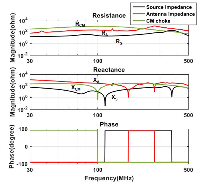
Figure 7: Impedance Curve of a CM Inductor
Figure 8 compares the KI and KE curves before and after adding a CM inductor. The CM inductor reduces KI and KE by about 13dB.
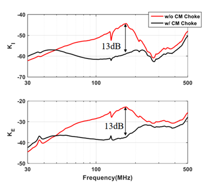
Figure 8: Comparison of KI and KE with or without CM Inductors
Figure 9 shows the test results of IA (on the left) and radiated EMI (on the right) both with and without an CM inductor in the circuit.
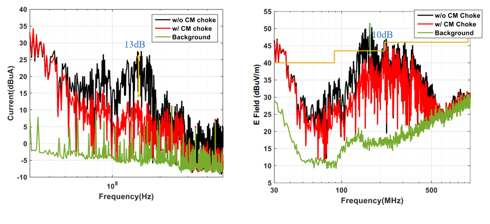
Figure 9: Comparison of CM Current and Radiated EMI with and without a CM Inductor
These results indicate that adding a CM inductor can suppress the previous spikes in EMI. The actual results are also aligned with the KI and KE variations. After adding a CM inductor, the noise at 167MHz meets the FCC Class B radiated EMI standard, but the margin is small. At 30MHz, the noise remains above the standard.
Impact and Design Methodology when Using a Y-Capacitor for Radiated EMI
Other filter components for suppression can be considered, such as a Y-capacitor. Connecting a Y-capacitor across the input and output DC buses is another popular method to suppress EMI. Similar to the inductor model, the Y-capacitor model can be expressed as a series form of equivalent series resistance (ESR, represented as RY) and reactance (XY) (see Figure 10).
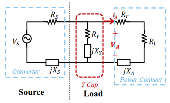
Figure 10: Radiated EMI Model Considering Y-Capacitance
In general, the Y-capacitor’s RY is negligible and can be ignored. In addition, EMI noise can only be bypassed when the Y-capacitor’s impedance is significantly smaller than the antenna impedance. Thus, we can assume that XY << XA. Under these assumptions, the modified current coefficient (KI_Y) and electric field intensity coefficient (KE_Y) can be obtained.
KI_Y can be calculated with Equation (8):

KE_Y can be calculated with Equation (9):

EMI Reduction at 30MHz and 167MHz
Due to the need to further suppress EMI noise at 30MHz and 167MHz, analysis can be conducted under these two frequency bands.
Based on the impedance curve in Figure 3, XA >> RA, XS, and RS at 30MHz. By comparing KI_Y and KI (or KE_Y as can be observed from KE), the insertion loss of the Y-capacitor is calculated with Equation (10):

To effectively suppress EMI, the insertion loss must be below 1, where a smaller value indicates a better effect on EMI. This means that |XY| must be below |XS|, and |XY| must be as small as possible. According to the measurements in Figure 3, if XY is capacitive at 30MHz, its capacitance must exceed 86pF to ensure that the insertion loss is below 1; if XY is inductive at 30MHz, its inductance must be below 327nH to ensure that the insertion loss is below 1.
At 167MHz, the impedance curve indicates that RA >> XA, XS, and RS. Through simplification, insertion loss is consistent with Equation (10). A similar analysis indicates that if XY is capacitive at 167MHz, its capacitance should exceed 30pF; if XY is inductive at 167MHz, its inductance should be below 30nH.
Figure 11 shows two feasible Y-capacitors and their impedance curves by combining the requirements for both frequency bands. The blue curves on the left show a 100pF Y-capacitor, while the black curves on the right show a 470pF Y-capacitor. At 30MHz, the 470pF capacitor has a lower impedance, which is better for EMI suppression. At 167MHz, the 100pF capacitor demonstrates better performance.
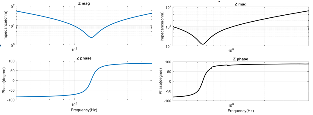
Figure 11: Impedance of Y-Capacitor at 100pF (Blue) and 470pF (Black)
Figure 12a shows a comparison of the effects of different Y-capacitors on the KI and KE coefficients. Both the 100pF and 470pF Y-capacitors can effectively suppress EMI. Moreover, the 100pF capacitor has a significant effect in the 167MHz frequency band, while the 470pF capacitor is more effective in the 30MHz frequency band. This is also consistent with the previous theoretical analysis.
Figure 12b shows the EMI measurement results that further validate the theoretical analysis. When using different Y-capacitors, the radiated EMI decreases to varying degrees in different frequency bands, and this reduction is consistent with the predicted results. From these results, it can be seen that for the design of radiated EMI, the filtering element can be adjusted to suppress a specific frequency band.
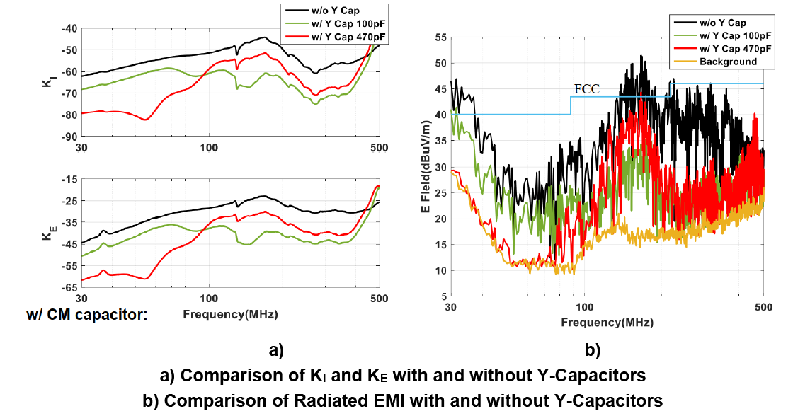
Figure 12: Comparing KI, KE, and Radiated EMI
Principles of LC Filter Design
When both the inductor and capacitor filter components are present in the circuit (see Figure 13), the design should follow the impedance mismatch principle. If the source impedance is small, use a filter inductor with a large impedance in series; if the load impedance is large, connect a bypass capacitor with a small impedance in parallel.
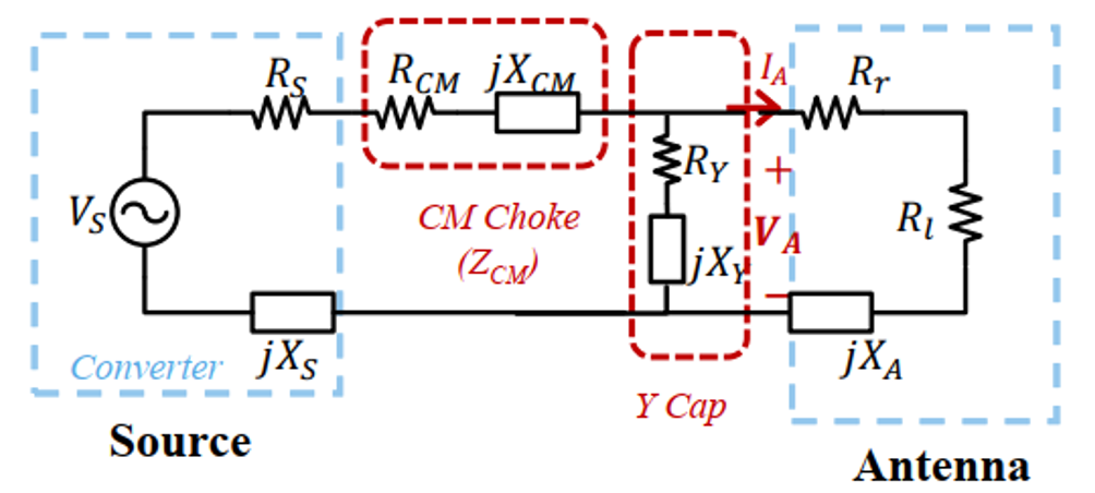
Figure 13: Radiated EMI Model with both the Inductor and Capacitor as Filter Components
Conclusion
This article reviewed the basic model of radiated EMI and introduced the principle of generating radiated EMI spikes. Then we considered a dual active bridge converter to observe how CM noise can be impacted by the CM inductor and Y-capacitor.
In the conduction frequency band, the low-frequency characteristics of the filter elements are typically used to suppress EMI. In the radiation frequency band, the stray parameters of the filter elements are typically used to achieve EMI suppression more effectively.
MPS offers a complete line of isolation solutions that are optimized for demanding industrial and automotive environments. Using capacitive isolation, MPS’s isolated products minimize supply current and achieve high CMTI as well as high immunity to magnetic noise.
_______________________
Did you find this interesting? Get valuable resources straight to your inbox - sent out once per month!
Technical Forum
 Latest activity 8 hours ago
 1 Comment
Latest activity 8 hours ago
3 Comments
Latest activity 2 days ago
2 Comments
1 Comment
Latest activity 8 hours ago
3 Comments
Latest activity 2 days ago
2 Comments
Log in to your account
Create New Account