Using External Knobs to Improve Transient Performance of Buck Regulators with an Integrated Compensation Network

Get valuable resources straight to your inbox - sent out once per month
We value your privacy
Introduction
The high power density requirement and board-level space constraints in modern applications — such as lighting, ADAS, and USB — call for higher integration in buck regulators. There is a trend to integrate MOSFETs and compensation networks inside the chip. This integration of the compensation network’s passive components saves cost, board space, and design iterations. However, it also limits the ability to further optimize the control loop for better transient response. This article will discuss how external knobs can be used to further optimize the transient performance of internally compensated buck regulators.
Quick Overview of Peak Current Mode (PCM) Control in Buck Regulators
One of the main advantages of peak current mode (PCM) control over voltage mode (VM) control is the fact that PCM control breaks the complex conjugate poles of VM control into two single poles, simplifying compensation network design. Figure 1 shows a typical PCM control buck regulator schematic and its bode plot.
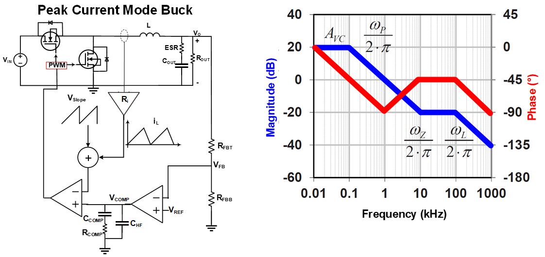
Figure 1: PCM Buck Regulator Schematic and Bode Plot
The two power stage poles, (ωP and ωL) in Figure 1 can be calculated with Equation (1) and Equation (2), respectively:
$$\omega_{P} \approx \frac {1}{C_{OUT} \space x \space R_{OUT}} $$ $$\omega_L = {K_m \space x \space R_i \over L} $$Where Ri can be calculated with Equation (3):
$$R_i = A \space x \space R{s}$$And Km can be calculated with Equation (4) when D = 0.5 (D representing the duty cycle):
$$K_m \approx {V_{IN} \over V_{SLOPE}}$$The single zero (ωZ) in the power stage bode plot can be estimated with Equation (5):
$$\omega_Z = {1 \over C_{OUT} \space x \space ESR}$$Evaluating the Internal Compensation Networks
The internal Type II compensation network in buck regulators include a zero/pole pair (see Figure 2).
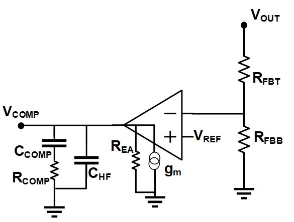
Figure 2: Type II Compensation Network and Zero/Pole Locations
The Type II compensation network’s zero frequency and pole frequency can be calculated with Equation (6) and Equation (7), respectively:
$$\omega_{COMP}-Z1 = {1 \over R_{COMP} \space x \space C_{COMP}}$$ $$\omega_{COMP}-P1 = {1 \over R_{COMP} \space x \space C_{HF}}$$For a proper tradeoff between bandwidth (BW) and phase margin (PM) in PCM buck regulators, the BW is normally set at 10% of the switching frequency (fSW), calculated with Equation (8):
$$BW = 0.1 \space x \space f_{SW}$$To achieve the maximum available PM, the compensation network zero (COMP-Z1) must be placed between 10% and 20% of the BW, so it can provide its maximum phase boost at the BW frequency. This relationship can be demonstrated with Equation (9):
$$0.1 \space x \space BW < f_{COMP-Z1} $$The compensation network pole (COMP-P1) provides noise attenuation at higher frequencies. In practice, the assumption calculated with Equation (10) can be used as a good rule of thumb for the COMP-P1 frequency:
$$f_{COMP-P1} = f_{SW} / 2$$Having COMP-Z1 and COMP-P1 both in terms of the switching frequency results in a relationship between CCOMP and CHF, calculated with Equation (11):
$$C_{HF} < 4\% \space x \space C_{COMP}$$Additional Knobs to Further Optimize the Internal Compensation Networks
There are two effective ways to further optimize the transient performance of a buck regulator’s internal compensation network. One is to add a resistor in series with the feedback (FB) pin. The FB series resistor changes the BW by shifting the magnitude curve up and down, without significantly affecting the phase curve. Higher resistance in this resistor corresponds with a lower BW. It is recommended to place a 0Ω resistor in series with the FB pin in the initial design, so it can be changed if needed.
The next component, which can be effectively used to increase the PM, is the feed-forward capacitor (CFF). This capacitor is added in parallel with RFBT in the feedback divider and makes a second zero in the compensation network, making it Type III (see Figure 3).
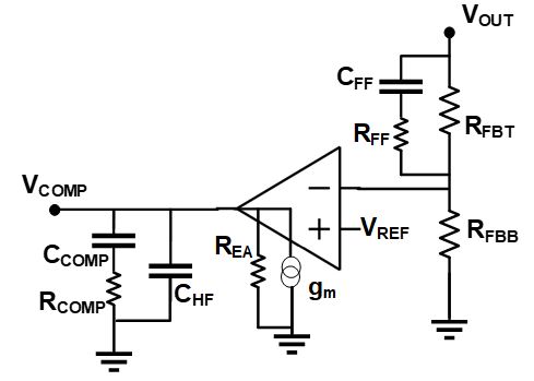
Figure 3: Type III Compensation Network Schematic and Zero/Pole Locations
The frequency of the zero created by CFF can be calculated with Equation (12):
$$\omega_{COMP}-Z2 \approx {1 \over R_{FBT} \space x \space C_{FF}}$$Placing RFF in series with CFF adds an additional pole to the compensation network. This pole can be used to provide additional attenuation at higher frequencies. The frequency of this pole can be calculated with Equation (13):
$$\omega_{COMP}-P2 \approx {1 \over R_{FF} \space x \space C_{FF}}$$Systematic Approach to Optimize the Compensation Network in PCM Buck Regulators
Based on the points discussed above, here is a systematic approach to evaluate and optimize internal compensation networks:
- Set the regulator target BW to 0.1 x fSW.
- Calculate the internal COMP-Z1 frequency with Equation (6), and ensure it meets the target set by Equation (14): $$0.1 \space x \space BW < f_{COMP-Z1} < 0.2 \space x \space BW$$
- Ensure that the requirement set by Equation (15) is met: $$C_{HF} < 4\% \space x \space C_{COMP}$$
- Run the initial bode diagram once the power stage design is complete. Ensure that:
- The BW is close to the target (at 0.1 x fSW).
- The phase starts descending at the target BW and not prior.
- If the BW measured in step 4 was not close to the target BW specified in step 1, adjust the FB series resistor so that the BW aligns with the target.
- Rerun the bode diagram and check the PM to ensure that it exceeds 60° with the FB series resistor. If it does, ignore the following steps. If it does not, proceed with steps 7 through 10.
- Set CFF such that the COMP-Z2 frequency is near the value calculated with Equation (16): $$0.2 \space x \space (target\space BW) < f_{COMP-Z2} < 0.4 \space x \space (target\space BW)$$
Measure the bode diagrams again, and confirm that the maximum phase boost on the phase diagram aligns with the target BW frequency.
- Tune/increase the FB series resistor to bring the BW back to its original target value, since CFF changed the magnitude curve in the previous step.
- The target BW (at 0.1 x fSW) and the target PM (>60°) should have been achieved.
- Optional: For higher attenuation at higher frequencies (HF), add a resistor (RFF) in series with CFF (see Figure 3). This creates a second pole (COMP-P2). To properly set the COMP-P2 frequency (fCOMP-P2), estimate the minimum ESR zero frequency with Equation (5) and fSW / 2, then set the lower of the two as the target for the COMP-P2 frequency. Start with an RFF value that brings COMP-P2 to its target value. Note that the negative phase due to this pole will come into effect at 0.1 x fCOMP-P2, and may slightly reduce the PM.
The procedure above can also be applied to parts with external compensation networks. In that case, RCOMP, CCOMP, and CHF should be selected such that the requirements in Equation (14) and Equation (15) are met.
Case Study – The MPQ4420
Let’s look at a real-world example to illustrate this principle. The MPQ4420 from MPS is a 36V, 2A, synchronous step-down converter with integrated MOSFETs and an integrated compensation network, which has a default 400kHz fixed switching frequency. Figure 4 shows the typical application schematic and the internal error amplifier for the MPQ4420.
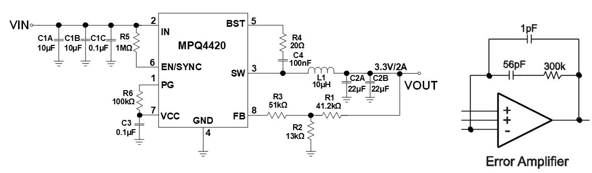
Figure 4: MPQ4420 Schematic and Internal Compensation Network Architecture
Let’s apply the step-by-step approach. Refer to Table 1 and Figure 5, and follow the steps below:
- Since the switching frequency is 400kHz, the target BW is set at 10% of that value, which is 40kHz.
- Calculate the COMP-Z1 frequency with Equation (6). This result is a COMP-Z1 of about 9.5kHz. This is close enough to the target COMP-Z, which should be between 4kHz and 8kHz based on Equation (14).
- Compare CHF to CCOMP. Based on Figure 4, CHF and CCOMP are 1pF and 56pF, respectively. Therefore, CHF is about 2% of CCOMP. This meets the requirement set by Equation (15).
- Simulate the bode diagram of the whole schematic (including the power stage components). Figure 5(a) and Table 1 show the bode measurement result. The BW is 72kHz, which exceeds the 40kHz target. On the other hand, the phase starts descending at about 40kHz, which meets the target expectation.
- Increase the FB series resistor. R3 in Figure 4 shows the FB series resistor. Typical values are between 10kΩ and 100kΩ. Increase the FB series resistor value in steps of 5kΩ until the target BW is achieved. In this example, the target BW is achieved with a 15kΩ FB series resistor.
- Compare the PM achieved by step 5 to the target PM, which should exceed 60°. As shown in Table 1, the PM is only 34°. Therefore, additional phase boost is required to achieve the target PM.
- Add the second compensator (COMP-Z2) to provide additional phase boost at the BW frequency. The CFF value calculated in Equation (12) is 220pF. Figure 5(b) shows the bode measurement results after the additional phase boost is added to the system. The maximum phase boost occurs around the 40kHz target BW.
- Change/increase the FB series resistor to return the BW to its target value (40kHz) since adding CFF/COMP-Z2 increased the BW to 104kHz. Figure 5(c) shows the bode measurement results.
- Ensure the system is optimized with a BW of 40kHz (0.1 x fSW) and a PM the exceeds 60°. Both targets should have been achieved.
- To provide higher attenuation above the switching frequency, add RFF in series with CFF to make the second pole (COMP-P2). Since the switching frequency is 400kHz < 1MHz, fSW / 2 is set as the target frequency to locate COMP-P2. Knowing the target fCOMP-P2 and CFF, the initial value of RFF should be 3.6kΩ.
Figure 5(d) shows the bode measurement result after step 10. As observed here, the slope of the magnitude curve and phase curve have both increased slightly above the BW, which means higher attenuation for noises above the BW frequency.
The summary of step 10 results (see Table 1) show that the higher attenuation above the BW frequency is achieved at the expense of reducing the PM by 6°, even though the PM still exceeds 60°, which was the initial target. If the 6° reduction in the PM is not desirable, use a smaller RFF value to regain some of the lost PM.

a) Step 4 to Step 5

b) Step 5 to Step 7

c) Step 7 to Step 8

d) Step 8 to Step 10
Figure 5: Bode Measurements of the MPQ4420 for Compensation Network Design
| Step 4 | Step 5 | Step 7 | Step 8 | Step 10 | |
| FB Series Resistor | 0Ω | 15kΩ | 15kΩ | 51kΩ | 51kΩ |
| CFF | NP | NP | 220pF | 220pF | 220pF |
| RFF | NP | NP | NP | NP | NP |
| BW | 72kHz | 41kHz | 104kHz | 40kHz | 38kHz |
| PM | 12º | 34º | 44º | 78º | 72º |
Table 1: Summary of MPQ4420 Compensation Network Optimization
MPQ4420 Transient Performance Verification
Figure 6 shows how to verify that the MPQ4420’s compensation network parameters are optimized. The output voltage is nominally set to 3.3V. When load transition occurs, the output voltage (VOUT) has an overshoot/undershoot of less than 2%, then returns to its nominal value. The absence of ringing on VOUT during the load transition confirms the system is stable with proper PM.
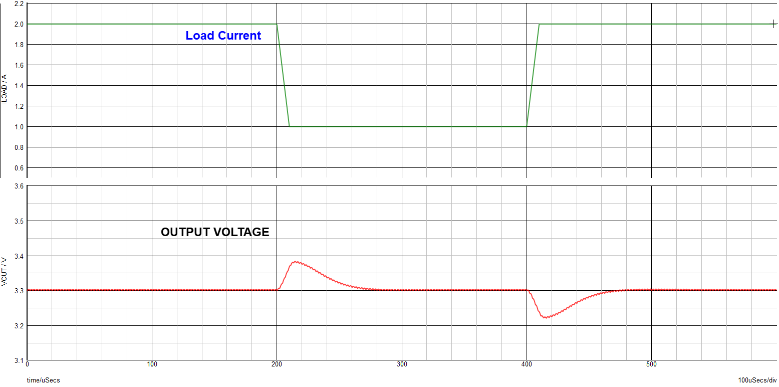
Figure 6: Transient Response of the MPQ4420 with Optimized Compensation Network
Conclusion
In this article, a systematic approach has been provided to further optimize the transient performance of internally compensated buck regulators, demonstrated with the MPQ4420. There are three main advantages associated with the proposed approach. First, this step-by-step approach limits the number of required iterations. Second, in each step of the proposed technique, only one parameter is changed to simplify optimization. Third, this method has minimal to no dependency on the power stage components, especially at switching frequencies below 1MHz.
_______________________
Did you find this interesting? Get valuable resources straight to your inbox - sent out once per month!
Technical Forum
 Latest activity 3 years ago
 2 Comments
Latest activity 2 years ago
2 Comments
Latest activity 6 years ago
4 Comments
2 Comments
Latest activity 2 years ago
2 Comments
Latest activity 6 years ago
4 Comments
Log in to your account
Create New Account