Understanding LLC Operation (Part II): What to Consider in LLC Converter Design

Get valuable resources straight to your inbox - sent out once per month
We value your privacy
Introduction
Designing an LLC converter involves a wide range of design decisions and key parameters, many of which are related. This means any single design choice impacts a multitude of other parameters in the system. The LLC tank in particular poses the greatest design challenge because it determines the converter’s capacity to respond to changes in load, frequency, and voltage. Therefore, designers must properly define the converter’s operating range regarding loads and frequencies, as these values influence the resonant tank’s values and parameters.
This is the second part of a two-part series discussing key considerations for designing an LLC converter. Part I explored various power switch topologies and the LLC resonant tank’s characteristics. Part II will cover the important parameters in LLC converter design, including gain, load, frequency, and inductance.
LLC Converter Gain
The two blocks in an LLC converter that affect gain are the resonant tank and transformer. The resonant tank’s gain is variable and depends on the load (Q), normalized frequency (fN), and normalized inductance (LN). The converter’s gain response (MG, as a function of (Q, LN, fN)) can be calculated with Equation (1):
$$M_G(Q,L_N,f_N) = \frac {V_{OUT(AC)}}{V_{IN(AC)}} = \frac {f_N^2 \times (L_N-1)} {(f_N^2 -1)^2 + (f_N^2 \times (f_N^2 -1) \times (L_N-1)^2 \times Q^2}$$The transformer’s gain is defined by the ratio of the number of turns in the transformer’s primary coil to the turns in the secondary coil. Because this ratio is defined by the physical construction of the transformer, it cannot be easily changed once the converter is operating.
Figure 1 shows the gain path of an LLC converter.
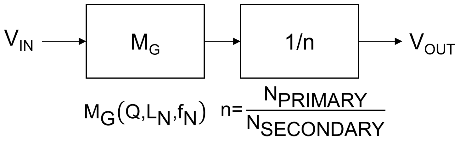
Figure 1: Gain Path of an LLC Converter
Figure 2 shows the schematic of an LLC tank with a transformer.
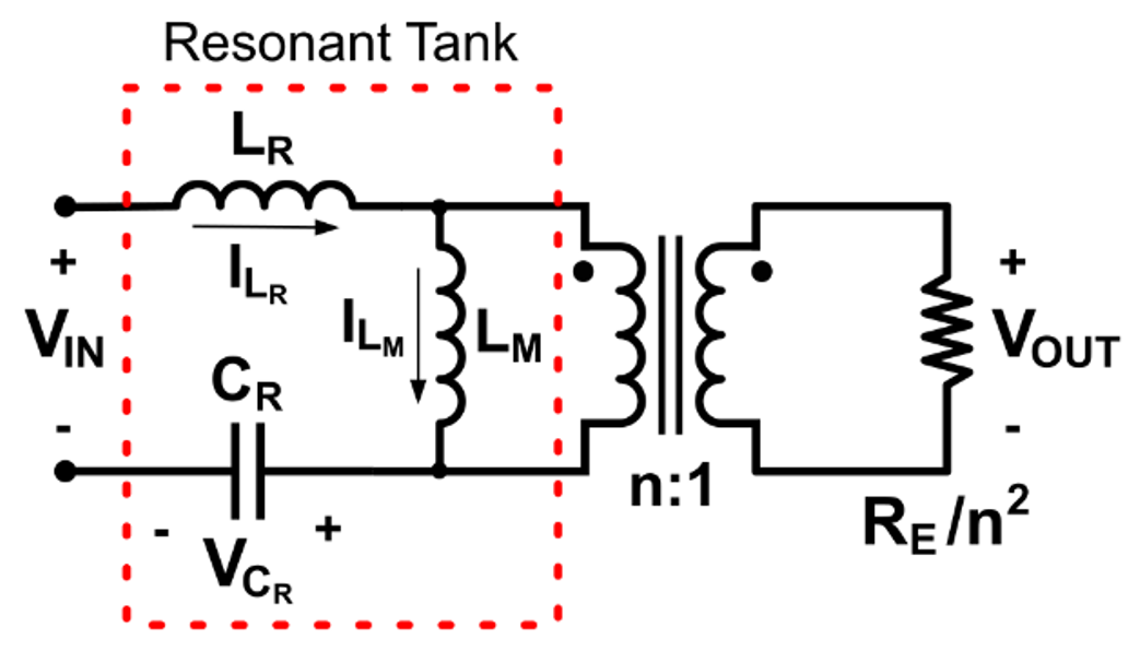
Figure 2: Schematic of an LLC Tank with a Transformer
The converter’s total gain (VOUT / VIN) is defined as the product of both gains. VOUT / VIN can be estimated with Equation (2):
$$\frac {V_{OUT}}{V_{IN}} = M_G \times \frac {1}{n}$$Where n is the transformer’s turn ratio and MG is the LLC tank’s gain.
Ideally, the resonant tank does not amplify or dampen the signal, but rather filters out the harmonics. This means the nominal gain of the resonant tank should be 1, and the transformer should be the only stage that changes the output voltage level.
In practice however, LLC converters are often used in AC/DC converters. Generally, an AC/DC converter is comprised of an AC/DC + PFC conversion stage and an LLC DC/DC converter to step the voltage down to the required level (see Figure 3).
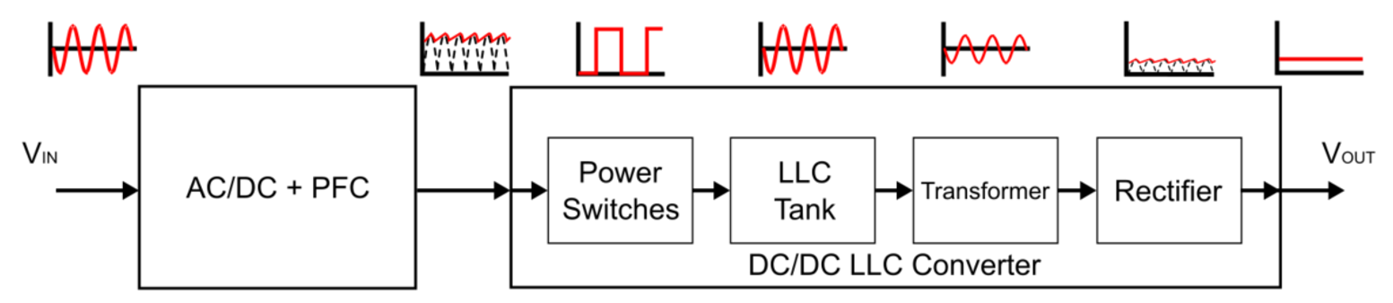
Figure 3: AC/DC Converter Block Diagram
The AC/DC + PFC stage converts the AC input voltage (VIN) (e.g. the power from the AC mains) into a stable DC voltage, while also keeping the input current in phase with VIN. This PFC stage is necessary to ensure that the design meets various power factor regulations imposed by international standards, including ISO, UNSCC, IEEE, and CISPR. The output voltage (VOUT) of the AC/DC + PFC stage is ideally stable, but a voltage ripple tends to occur at the AC/DC output due to the non-ideality of the components, which are often a result of parasitic inductance and the capacitor’s ESR. This voltage ripple is also present at the input of the LLC converter.
With the resulting variations in the converter’s VIN and the transformer’s fixed gain, the LLC tank must compensate for any VIN variations to obtain a constant VOUT. As a result, if VIN is below the nominal value, then the tank slightly amplifies the signal to produce the maximum resonant tank gain. If VIN exceeds the nominal value, the minimum resonant gain ensures that the voltage at the transformer’s primary winding remains at the nominal value required to maintain a stable VOUT.
The nominal resonant gain (MG_NOM) can be calculated using Equation (3):
$$M_{G\_NOM} = \frac {V_{OUT} \times n} {V_{IN\_NOM}}$$The maximum resonant gain (MG_MAX) can be calculated using Equation (4):
$$M_{G\_MAX} = \frac {V_{OUT} \times n} {V_{IN\_MIN}}$$The minimum resonant gain (MG_MIN) can be calculated using Equation (5):
$$M_{G\_MIN} = \frac {V_{OUT} \times n} {V_{IN\_MAX}}$$Figure 4 shows an LLC converter’s gain response with the required values for maximum, minimum, and nominal resonant tank gain.
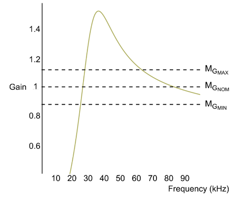
Figure 4: LLC Converter Gain Response
Related Content
-
REFERENCE DESIGN
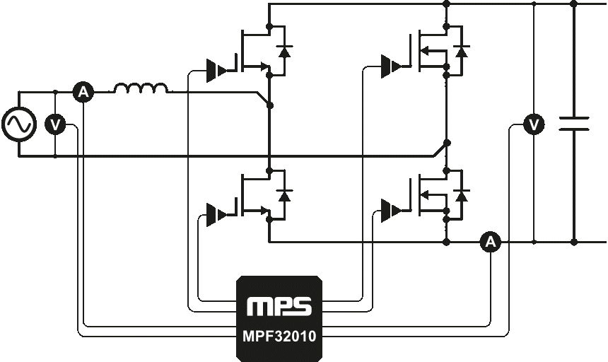
MPF32010 Totem-Pole Reference Design
The EVF32010-18831 evaluation board is an AC/DC power factor corrector based on totem-pole topology
-
VIDEO

Powering 5G: PFC + LLC Power Supply Solution
Powerful, efficient PSU for 5G telecom applications
-
ARTICLE

Digital PFC + LLC Combo Controller Helps Fast-Charge Adapters Enter the New Age
The HR1211's excellent efficiency, performance, power density, and flexibility will help the adapter market enter a new age
-
APPLICATION NOTE
AN145 - Multi-Mode PFC + Current Mode LLC Controller
The HR1211 is a combination controller that integrates multi-mode PFC and current Mode HB LLC controllers and exhibits very high performance
LLC Converter Load
As discussed in Part I, the load is expressed through the quality factor (Q), which impacts the tank’s maximum gain as well as the peak gain frequency. The resonant tank’s peak gain decreases as the load increases. This means that it is important to meet the maximum gain requirement — even in the worst-case scenario, where the load is at its highest.
Figure 5 shows the LLC converter frequency response for a series of loads.
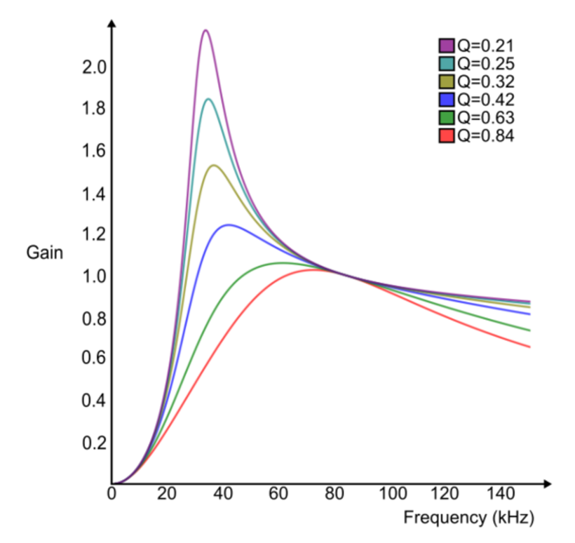
Figure 5: LLC Converter Frequency Response
LLC Converter Switching Frequency
Since the effect of load on the gain cannot be controlled, the circuit’s gain is maintained by changing the switching frequency (fSW) of the MOSFETs. Figure 5 shows that although the load affects the converter’s maximum gain, increasing the load also drags the frequency, at which the maximum gain is produced (fMG_MAX) to higher levels.
Figure 6 shows the maximum gain points for a series of different loads in an LLC tank plotted into a dotted line. This line divides the gain response into two distinct regions. In the inductive region (right), zero voltage switching occurs, and the gain increases as frequency decreases until the peak gain frequency is reached. Then the converter enters the capacitive region (to the left of the peak gain frequency) where reducing the frequency also reduces the gain. The inductive region allows for stable gain control through changes in the frequency.
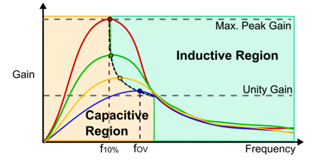
Figure 6: Capacitive and Inductive Regions of Frequency Response
Entering the capacitive region is not recommended due to the possibility of the high-side MOSFET (HS-FET) (S1) turning on while the low-side MOSFET (LS-FET) (S2) transistor’s body diode is in reverse recovery (see Figure 7). This scenario creates a potential shoot-through condition for the half-bridge, which can result in the failure of S2, or at the very least, reduce the converter’s efficiency.
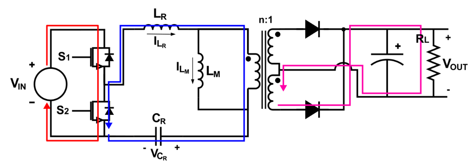
Figure 7: Shoot-Through Current in the Power Switches
Different loads generate different frequency responses and maximum gain frequencies. To establish the minimum fSW, consider the worst-possible scenario, when the load shifts from lightest load to the heaviest load (see Figure 8). When the load is light, the converter operates in the inductive region, but if the load suddenly increases, the operating point enters the capacitive region. As such, the minimum frequency (fMIN) should increase to ensure that the operating point remains in the inductive region for all loads.
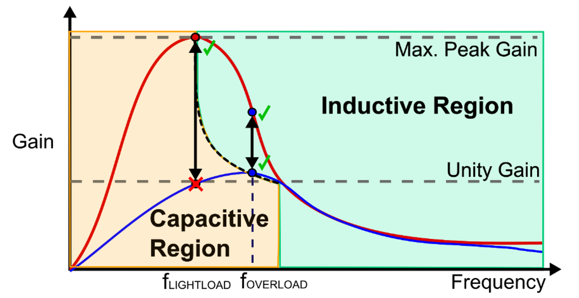
Figure 8: Impact of Load Shift on Operating Region
Thus, to establish a stable frequency range, fMIN must be equal to the converter’s maximum gain frequency in an overload situation (fOVERLOAD) (see Figure 9).
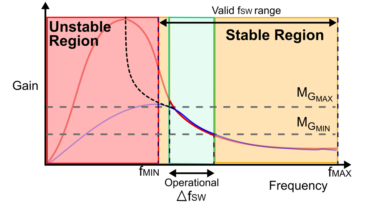
Figure 9: Switching Frequency Ranges of Stable, Unstable, and Operational Frequency Windows
Once the converter’s minimum frequency is obtained, an operational fSW range can be established. The converter’s maximum frequency (fMAX) is limited by the controller’s and the MOSFETs’ maximum frequencies. However, the operating window does not need to very large, and can instead be defined through the maximum and minimum gain frequencies, provided that they are in the stable frequency range.
LLC Tank Inductance
Figure 10 shows that the normalized LN defines the peak gain slope that marks the limit between the inductive and capacitive regions. For the same load, the tank’s peak gain depends on the normalized LN.
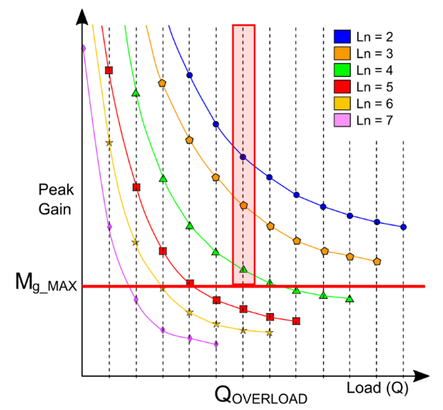
Figure 10: Maximum Gain Curves of an LLC Converter with Different Normalized Inductances
A smaller LN provides high gains for a wider range of loads and operations. On the other hand, a smaller LN also results in a higher magnetizing current and lower efficiency.
To select an adequate value for the normalized LN., the designer must consider the worst-case scenario when the load is at its heaviest. LN must be selected so that it can deliver sufficient gain to compensate for any shortcomings in VIN, even in under overload conditions.
Conclusion
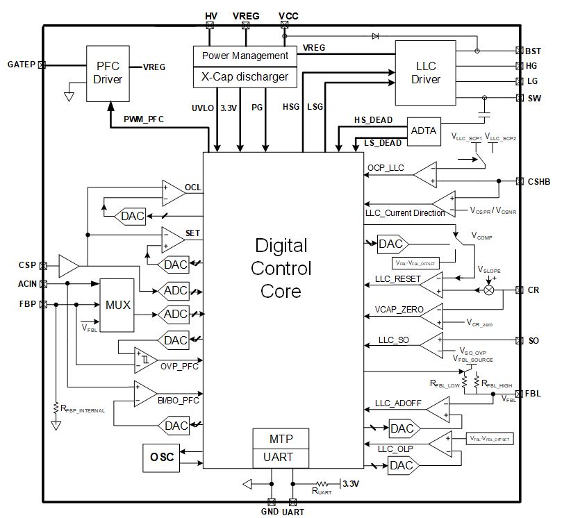
Designing an LLC converter is a long and complex process that involves a myriad of considerations according to the specific application requirements. Due to the large number of parameters and the relationships between these parameters, the design process typically spans many iterations and calculations that can lead to lengthy design times. MPS offers tools such as the MPS LLC Designer and the MPF32010, a configurable LLC controller, to significantly accelerate the development process.
_______________________
Did you find this interesting? Get valuable resources straight to your inbox - sent out once per month!
Technical Forum
 Latest activity a month ago
 2 Comments
Latest activity a month ago
2 Comments
Latest activity 2 months ago
2 Comments
2 Comments
Latest activity a month ago
2 Comments
Latest activity 2 months ago
2 Comments
Log in to your account
Create New Account