MPS Power Modules Offer A Compact and Ultra-Low Noise Solution for AMD Xilinx Zynq UltraScale+ RFSoC
By Heng Yang, Ph.D., Sr. Applications Engineer MPS
The growing number of high-performance FPGA and ASIC applications that are driven by the increased bandwidth of wireless networks and data centers demand for power regulators with high power density, fast load transient response, and high efficiency. AMD Xilinx Zynq UltraScale+ RFSoCs integrate multi-giga-sample RF data converters and soft-decision forward error correction (SD-FEC) into a SoC architecture. Complete with an ARM Cortex-A53 processing subsystem, UltraScale+ programmable logic, and the highest signal processing bandwidth in a Zynq UltraScale+ device, the new family provides a comprehensive RF signal chain for wireless, cable access, test & measurement, early warning / radar, and other high performance RF applications. However, the higher degree of integration of the Zynq UltraScale+ RFSoC poses challenges for power solution design. In addition, the performance of the RF data converters is closely coupled with the noise level of their power supplies. MPS Power modules offer both high efficiency operation and minimized board space. This application note outlines the power solution design for a AMD Xilinx Zynq UltraScale+ RFSoC. The EVREF0102A reference design power supply, which is designed to provide ultra-low noise voltage for the RF data converters, is demonstrated.
Power Architecture
The power architecture of the Zynq UltraScale+ RFSoC is shown in Figure 1. As shown in the figure, more than 30 power rails are required for the RFSoC. The power rails in the PL domain are for the RFSoC, and the power rails in the PS domain are for the embedded arm core. The power rails are consolidated to minimize the required number of converters. The MPS power module solution minimizes the PCB space and simplifies the power supply design.

Figure 1. MPS Power Solution for Zynq UltraScale+ RFSoC
The current specification of each rail can vary depending upon the part number and specific application/program that will be running on the RFSoC. Table 1 illustrates the typical current requirement of each rail for the Zynq UltraScale+ RFSoC family. It is recommended to use the AMD Xilinx Power Estimation (XPE) tool to estimate the accurate current requirement
for optimization of the power solution design. Besides the voltage and current specifications, the power supplies for AMD Xilinx FPGA power rails must meet the following requirements:
- The output voltage ripple of all power rails (except for analog rails) must be smaller than 10mV in steady state.
- The start-up of all power rails must be monotonic.
- Output voltage deviation of the core rail (VCCINT) must be smaller than +- 3% during a 25% load transient at 100A/μs.
- The turn-on and turn-off of the power supplies must follow a certain sequence defined by AMD Xilinx.

*Supports up to 6V input voltage , **Supports 12V input voltage. Click for Complete Discrete Solutions.
Table 1. MPS Power Module Solution for AMD Xilinx Zynq UltraScale+RFSoC
Realization of Optimized Power Solution with Power Modules
MPS power modules offer a highly integrated power solution with high efficiency. Figure 2 illustrates the typical structure of MPS’ power modules, which integrates the MPS patented monolithic IC, inductor, and selected passive components in a single molded package. The components are mounted on a lead-frame using Mesh-connect packaging technology, which minimizes thermal resistance between the power IC/inductor, and the PCB. The monolithic IC integrates power FETs, a control circuit, and a driver on a single silicon die. Monolithic technology minimizes the parasitic resistance and inductance between the driver circuit and the gate of the power FET. Subsequently, the switching losses are minimized.
Table 1 shows the MPS power module solution for the AMD Xilinx Zynq UltraScale+ RFSoC. Note that a discrete solution is available from MPS.

Figure 2. Typical Structure of MPS Power Modules
Figure. 3 demonstrates the reference design board for the AMD Xilinx Zynq UltraScale+ RFSoC (exclude the RF data converter rails). The reference design board employs 5 advanced power modules. The MPM3695-25 is a 16V, 20A power module. The core rail utilizes two MPM3695-25s, which are connected in parallel to provide up to 50A peak current. A single MPM3695-25 provides up to 25A peak current for rail 2. The MPM3695-10 is a 14V, 7A ultra-thin power module. The MPM3632C is a 18V, 3A forced CCM power module.

Figure 3. Reference Design Board for Zynq UltraScale+RFSoC

Figure 4. Power-Up and Down Sequence
The MPM3606A is a 21V, 0.6A power module. The same family also offers pin compatible power modules with 1A, 2A, and 3A power modules, which provide great flexibility in power solution design. The performance of the reference design is fully verified to meet AMD Xilinx requirements. Figure 4 shows the waveform of the power-on and off sequence.
The advanced MPM3695 series of power modules with integrated inductors offer a versatile solution for powering FPGAs and ASICs. The output current of the MPM3695 series is scalable by stacking multiple MPM3695-25s or MPM3695-10s. The MPM3695 series offers up to 60% higher power density, compared to discrete point-of-load (POL) solutions, simplified PCB layout and power stage design, minimal external components, and minimal expertise for the power converter and compensation network design. With the monolithic structure of the power IC and customized integrated inductor design with advanced packaging technology, the MPM3695 series power modules reduce the footprint up to 40% compared to competing power modules.
Figure 5 and 6 show the load transient waveform at 25% load transient at 100μA/s and the output voltage ripple at full load, respectively. As shown in the figures, the output voltage deviation is below ± 3% during the load transient, and the output voltage ripple is smaller than 10mV at steady state.

Figure 5. Load Transient Waveform of the Core Rail.

Figure 6. Output Voltage Ripple of the Core Rail.
Analog Power Module for ZCU1275
The AMD Xilinx Ultrascale+ RFSoC embeds a highspeed analog to digital converter (ADC) and digital to analog converter (DAC), which require ultra-low output noise. A switch-mode power supply (SMPS) has the advantage of high efficiency compared to traditional low-dropout (LDO) regulators. Due to its switching nature, a SMPS emits noise at its switching frequency
and its harmonics. The MPS power module solution leverages two-stage CLC filters to minimize the output voltage noise for the sensitive ADC and DAC rails. The EVREF0102A is the RF data converter power module developed for the ZCU1275 Zynq UltraScale+ RFSoC Characterization Kit. Figure 7 demonstrates the EVREF0102 power module.

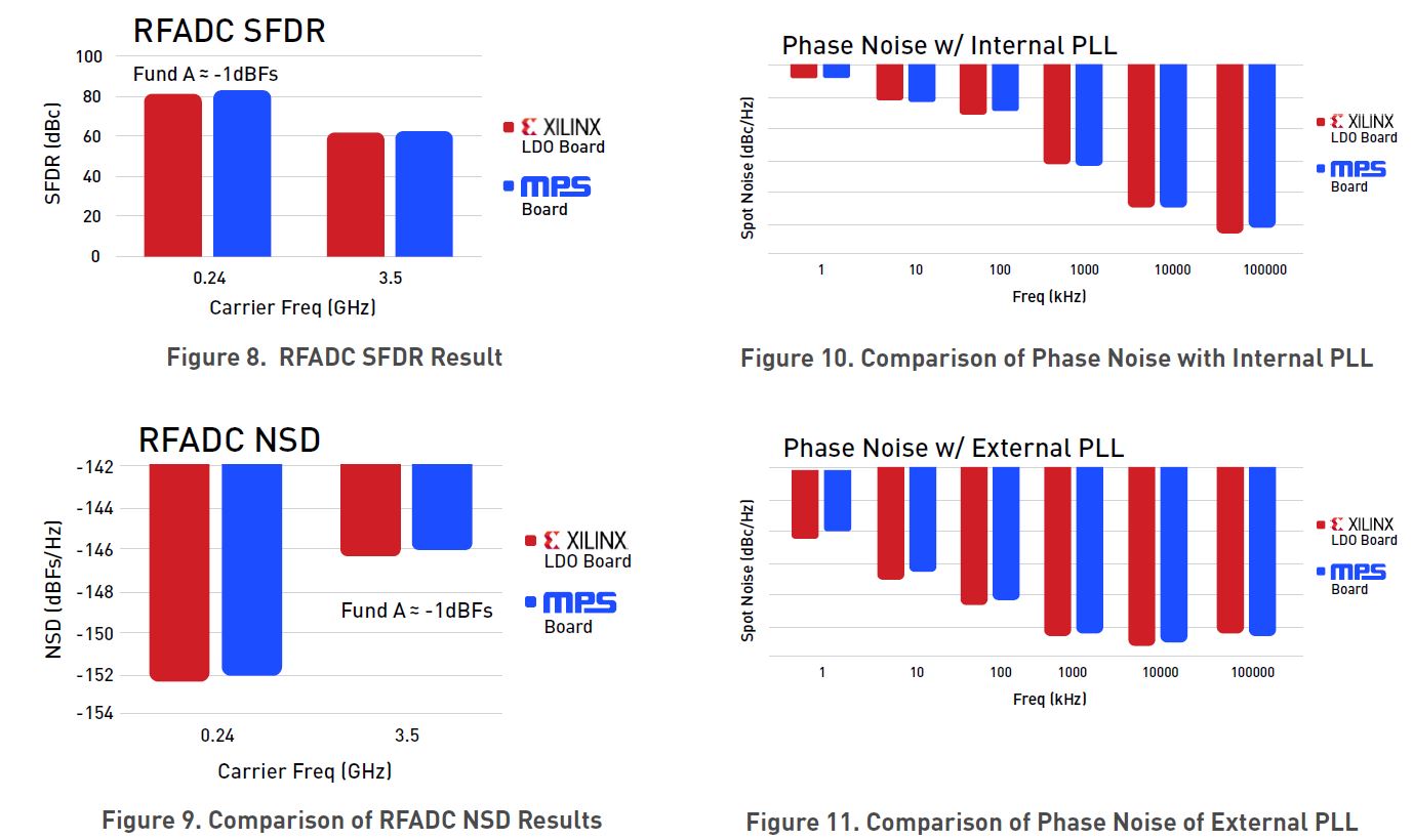
Figure 7. EVRF0102 Ultra-Low Noise Power Supply Module
The output voltage noise is below 1mV for all sensitive RF data converter rails. The EVREF0102A employs five high efficiency step-down switch-mode power modules with integrated inductors. The MPM3833C is a 6V, 3A, ultra-small step-down power module, and the MPM 3683-7 is a 16V, 8A power module. Both power modulesfeature integrated protection functions, including OCP, OVP, UVP, and OTP. Compared to the traditional LDO solution, the EVREF0102A can achieve up to an 80% efficiency improvement. The EVREF0102A analog power module also achieves ultra-low noise to meet the specifications of the AMD Xilinx high-speed data converter by leveraging the forced continuous conduction mode (CCM) operation and implementing post passive filters. CLC passive filters are utilized for the two most sensitive ADC and DAC rails, and capacitive filters are utilized for the rest of the power rails. See the Appendix for reference.
Figure 8-11 illustrate the comparison between the traditional LDO solution with the MPS power module solution. The experimental results were collected at a AMD Xilinx lab on the ZCU1275 development kit. As shown in the figures, the noise level of the MPS power module solution is comparable to the traditional LDO solution.
Conclusion
MPS power modules provide high efficiency, full integration, and a compact power solution for AMD Xilinx FPGAs. The scalable power module offers a versatile solution for the core rail. The efficiency is improved significantly by replacing the traditional LDO with power modules for the sensitive RF data converter power rails. Two reference design boards are available from MPS with fully verified performance. The design procedure of the passive filter for minimizing the output voltage ripple for the RF data converter rails is outlined in the appendix of this application note.
Appendix: Two-Stage Filter Design
A synchronous buck converter consists of an input capacitor (CIN), two switches (S1 and S2) with their body diodes, an energy storage power inductor (L), and output capacitor (COUT). The input source provides energy to the power inductor L and the load when S1 is turned on and S2 is turned off. During this period, the inductor current rises. The energy stored in the inductor is transferred to the output capacitor and load when S2 is on and S1 is off, causing the inductor current to drop. The switching behavior of the buck regulator causes the output voltage to fluctuate. The output capacitor COUT is placed at the output to smooth the output voltage under steady state. The output capacitor reduces the output voltage ripple by providing a low impedance path for the high-frequency voltage components to return to ground.

Figure 1: Low Noise Filter Design
In the subsequent development, it is assumed the buck converter operates under continuous conduction mode (CCM) for output voltage ripple minimization. The inductance of L is designed to meet the inductor current ripple requirement. The minimum inductance of L is determined as:
 (1)
(1)
Where VIN and VOUT represent the input and output voltage, respectively, D=VOUT/VIN represents the duty ratio, I_(L,p-p) is the peak-to-peak current ripple of the inductor, and fSW represents the switching frequency of the converter. Typically, the peak-to-peak inductor current ripple is selected as 20-40% of the output DC current.
The output capacitance is selected to ensure that the output ripple is below the specified peak-topeak value. For a single stage capacitive filter, a minimum output voltage ripple of 1mV to 2mV can be achieved.
Under steady state, the net electric charge delivered to the capacitor is zero within one switching period. The capacitor charge of the shaded area in Figure 1 is calculated as:
 (2)
(2)
Where T is the period of one switching cycle. By definition, the capacitor charge in a given period can also be expressed as:
![]() (3)
(3)
For equations (2) and (3), the minimum capacitance to achieve the required output peak-to-peak voltage ripple (VOUTp-p)is determined as:
 (4)
(4)
Ideally, the noise shunt capability can be increased by paralleling more output capacitors. In practical use, the output capacitors are placed laterally on a PCB. Adding more output capacitors on a PCB would introduce additional parasitic inductance and AC resistance to the shunt path and thus reduce the effectiveness of bypassing the switching noise.
A typical PCB layout of a MPS power module, which integrates optimized inductors to simplify the power converter design, is shown in Figure 2. In the PCB layout of the MPM3833C, a wide copper plane is used for the output power path to minimize power losses. The output capacitors are placed along the output current path. As shown in the figure, as more capacitors are placed on the output plane, the distance from the additional capacitor to the output pin of the power module increases. Consequently, more parasitic inductance is involved in the output capacitor that is farther away from the power module. Adding more output capacitance become less and less effective, and eventually, the shunt loop is dominanted by parasitic inductance.

Figure 2. Typical PCB Layout for the MPM3833C Power Module
To demonstrate the impact of loop parasitic inductance, an MPM3833C with various output capacitors is simulated using Simplis. It is assumed that each additional output capacitor introduces an additional 0.5nH parasitic inductance to the bypassing loop. Figure 3 illustrate the output ripple of the power module with one 22uF capacitor. The bypassing capacitor effectively reduces the output ripple to around 3mV at 5V input, 1.2V output, and 2A load.

Figure 3 Output Voltage Ripple of the MPM3833C with One 22uF Output Capacitor
To further reduce the output voltage ripple, 1 additional 22uF output capacitor is place at the output. Since the new capacitor has to be placed farther away from the power module, the parasitic inductance involved with the new capacitor is 1nH. The simulated output voltage ripple is shown in Figure 4 (a) where the output voltage ripple is reduced to 2mV. Compared to the waveform shown in Figure 3, where one 22uF output capacitor effectively brings down the output voltage ripple to 3mV, the additional 22uF capacitor is less effective. Fig. 4(b) shows the output voltage ripple with one more 22μF capacitor (total of 4x2μF). The last 22μF capacitor involves 1.5nH parasitic inductance in its bypassing loop. As shown in the figure, the output ripple reduction achieved by the additional 22μF capacitor is less than 5% compared to the case where 3x22μF is used.
 4x22uF Output Capacitors and (b) 5x22uF Output Capacitors")
Figure 4 Output Voltage Ripple of the MPM3833C with (a) 4x22uF Output Capacitors and (b) 5x22uF Output Capacitors
As demonstrated in Fig. 3 and Fig. 4, the parasitic inductance introduced by the PCB copper/trace will become dominant as more output capacitors are placed on the PCB. Eventually, the benefit of adding more capacitors will be negated by the additional parasitic inductance added in the loop.
Second Stage Filter Design
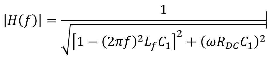
Typically, the shunt output capacitor can effectively reduce the output voltage ripple to 1mV. Beyond this point, a second stage output filter is required to achieve a smaller output voltage ripple (sub 1mV voltage ripple can be achieved). Fig. 5 illustrates a second stage LC filter, which is cascaded to the first stage output capacitors. The second stage filter consists of one filter inductor and its series resistor DCR, a bypassing capacitor branch, and a damping branch. The LC filter works by creating a high impedance to the output. The filtering inductor Lf is resistive at the intended high frequency range and dissipates the noise energy in the form of heat. The inductor combines with additional shunt capacitors to form a low-pass LC filter network.

Figure 5. Second Stage LC Filter with Parallel Damping Branch
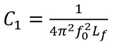
The second stage filter is very effective on reducing the output voltage noise when properly designed. It is crucial to size the component of the second stage LC filter for the intended frequency band. The first step of the design procedure involves choosing the first stage output capacitor based on Equation (4). 5mV to 10mV output voltage ripple is typical for the first stage design. Usually a 10-22uF capacitor is sufficient. The capacitor COUT of the first stage has to be smaller than the bypassing capacitor C1 of the second stage to ensure system stability.
Once the first stage capacitor COUT is determined, and the specified output voltage ripple (at given frequency) is given, the required attenuation of the second stage LC filter can be determined as:
 (5)
(5)
Where V1,p-p represents peak-to-peak voltage ripple at the output capacitor, and V0,p-p represents the peak-to-peak output voltage (after the second stage filter). Using phasor analysis, the amplitude of the gain of the LC filter is determined as:
 (6)
(6)
Note that the impedance of the damping branch, which consists a large series resistor, is much larger than the bypassing branch at the switching frequency. Thus the filter shown in Figure 5 is approximated as a second order RLC filter. The cut-off frequency of the filter is determined as:
 (7)
(7)
Typically, an inductor with 0.22μH to 1μH inductance can be selected to achieve the required output ripple. The inductor should be selected to have minimal DCR as the serious resistance increases power dissipation and reduces the output voltage regulation. It should be noted that as the DC current increases, the core material of the inductor becomes saturated, which reduces the inductance of the inductor. Care should be taken to ensure that the inductance is high enough at the rated DC current.
Once the filtering inductor is selected, its DCR can be extracted from the datasheet. The second stage LC filter, which is a second order filter, provides 40db per decade roll-off after the cutoff frequency. The attenuation at given frequency can be estimated as:
 (8)
(8)
Using the attenuation calculated in equation (5), the required cut-off frequency is determined as:
 (9)
(9)
Subsequently, the required bypassing capacitance C1 is determined as:
 (10)
(10)
Ceramic capacitors should be used as the bypassing capacitor for low ESR and ESL. It should be noted that the capacitance of ceramic capacitors experience significant de-rating at DC bias voltage. Figure 6 illustrates the DC de-rating curve of a Murata 0805 ceramic capacitor, which is rated at 6.3V. As shown in the figure, at the full rated DC bias voltage, the capacitance drops to 20% of the nominal value. The bypassing capacitor should be selected at the nominal DC bias voltage to factor in the de-rating.

Figure 6. Typical Ceramic Capacitor Derating Curve at DC Bias Branch
Damping
The second stage LC filter may introduce resonance peaking if not properly damped. The resonance between the filtering inductor and bypassing capacitor may amplify the output ripple and create undesired ringing at load transient. Figure 7 (a) shows the output voltage of an underdamped converter system with the second stage LC filter. Initially, the system operates under steady state. At t=200μS, a load transient from 1A to 2A is initiated, which causes the output voltage to ring. Figure 7(b) illustrates the output voltage and current under load transient of an overdamped second stage filter. To avoid undesired ringing at load transient, the second stage LC filter resonance must be properly damped. In most designs, the second stage filter will be placed outside of the control loop to avoid control stability issues. Consequently, the damping has to be achieved by passive components (additional damping resistors).
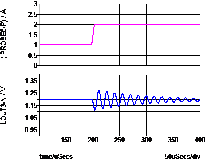
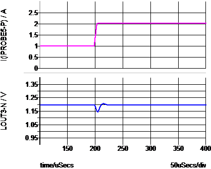
Figure 7. Step Response of (a) Underdamped LC Filter and (b) Overdamped LC filter
The filtering inductor usually includes a parasitic DC resistance in series with the inductor. This DCR provides damping to the network. However, to provide enough damping for a series RLC circuit, the series resistance has to satisfy 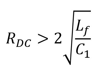 In most cases, the DCR alone cannot provide sufficient damping. To this end, a RC damping network is inserted in parallel with the bypassing capacitors to damp the resonant circuit along with the series DCR resistor.
mps-xilinx-artcile-q1-2019-_1.pdf
_____________________________________
Did you find this interesting? Get valuable resources straight to your inbox - sent out once per month!
Technical Forum
 Latest activity a day ago
 2 Comments
Latest activity a month ago
2 Comments
Latest activity a month ago
4 Comments
2 Comments
Latest activity a month ago
2 Comments
Latest activity a month ago
4 Comments
Log in to your account
Create New Account