Predictive Transient Simulation Analysis for the Next Generation of GPUs

Get valuable resources straight to your inbox - sent out once per month
We value your privacy
Introduction
Nowadays, graphics processing units (GPUs) feature tens of billions of transistors. With each new generation of GPUs, the number of transistors in GPUs continues to increase to improve processor performance. However, the growing number of transistors is also resulting in an exponential increase in power demand, which makes it more difficult to meet transient response specifications.
This article demonstrates how to use the SIMPLIS simulator from SIMPLIS Technologies to predict and optimize the behavior of power supplies for the next generation of GPUs, where high slew rate requirements and current levels exceeding 1000A demand faster transient response.
Constant-On-Time (COT) Control
The constant-on-time (COT) architecture of multi-phase buck converters replaces the error amplifier (EA) in the compensation network with a high-speed comparator. The output voltage (VOUT) is sensed via the feedback resistors and compared to a reference voltage (VREF). When VOUT drops below VREF, the high-side MOSFET (HS-FET) turns on. The MOSFET’s on time is fixed, meaning that the converter can achieve constant frequency in steady state. If there are load step transients, the converter can also significantly increase its pulse rate to minimize the output undershoot. In this scenario, however, the nonlinear loop control complicates loop tuning.
Figure 1 shows COT control for fast transient response.
Figure 1: COT Control for Fast Transient Response
The converter’s behavior and the power delivery network (PDN) must be accurately modeled to emulate the transient buck performance and validate various GPU-based systems without having to go through a long, costly iterative process.
Related Content
-
VIDEO

Non-Isolated, Two-Phase, Step-Down Intelli-Module for Server Applications: MPC22163-130
Core power intelli-module optimized for high-performance computing applications
-
ARTICLE
Powering the Next Sophisticated AI System
Artificial intelligence (AI) combines several approaches to problem solving, such as mathematics, computational statistics, machine learning, and predictive analytics.
-
VIDEO
Inside Xbox Series X: Engineering Design & Teardown of Power Delivery to SoC, GPU, CPU & Memory
Discover how MPS helps power the Xbox Series X
-
VIDEO
Tear Down of Nvidia RTX 3080 Power System
Youtube channel gamers NEXUS reviews the NVIDIA RTX 3080
Power Delivery Network (PDN)
The PDN is comprised of the components connected to the voltage and ground rail, including the power and ground plane layout, decoupling capacitors used for power stability, and any other copper features that connect or couple to the main power rails. The PDN design’s primary objective is to minimize the voltage fluctuations and ensure normal GPU operation.
Figure 2 shows the PDN architecture of a typical GPU power delivery network.
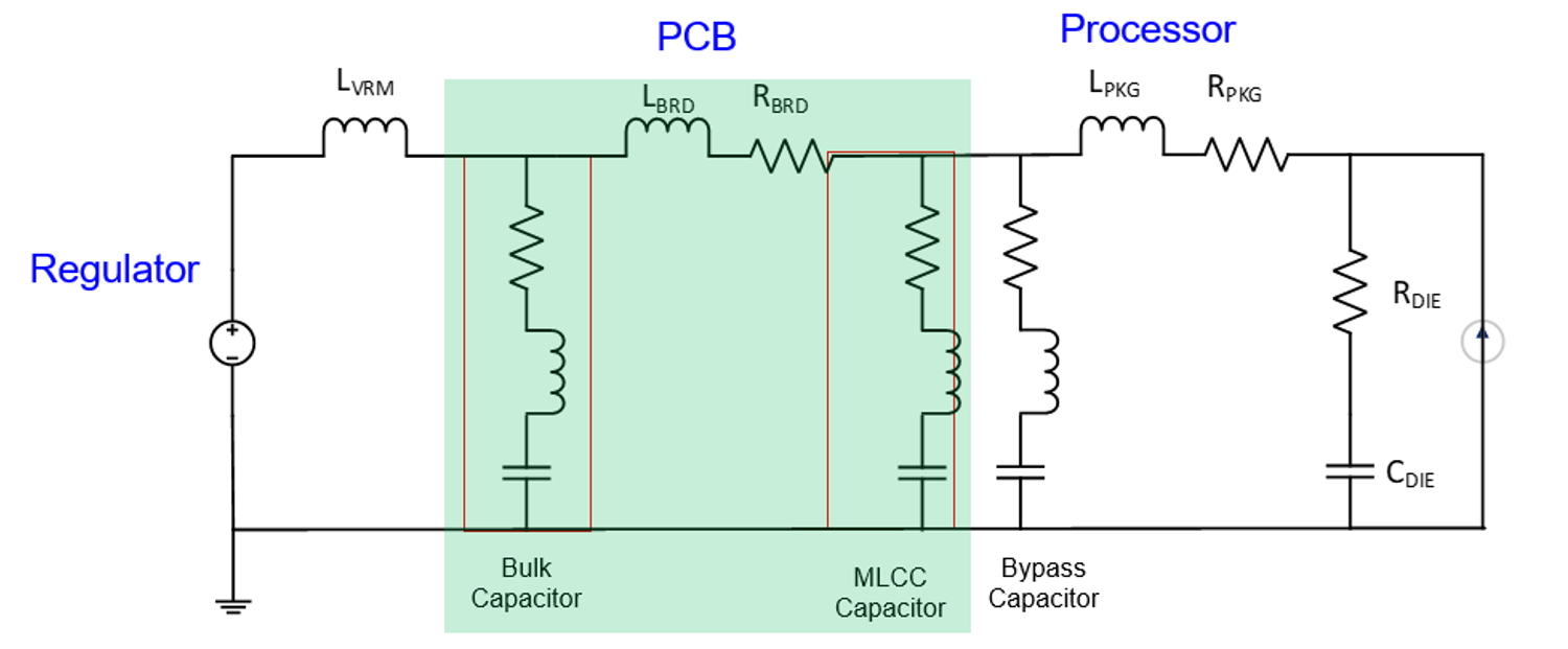
Figure 2: PDN Architecture of Typical GPU Power Delivery Network
The components in the PDN display parasitic behaviors, such as the equivalent series inductance (ESL) and equivalent series resistance (ESR) of the capacitor. These parasitic elements must also be considered when modeling the system response. Increasing the slew rates generates more powerful high-frequency harmonics. The PDN’s resistor, inductor, ad capacitor (RLC) components create resonant tanks that designers may not be aware of, with resonant frequencies that amplify the high-frequency harmonics created by the converter’s switching, leading to unexpected converter behavior.
Design Specifications
Table 1 shows the typical power rail requirements for artificial intelligence (AI) applications.
Table 1: Power Rail Specifications
| Parameter | Value |
| VIN | 12V |
| VOUT | 1.8V |
| IPEAK | 1000A |
| ISTEP | 300A (below 1µs) |
This analysis was made using an MPS evaluation board that combines the MP2891, a digital, 16-phase controller, and the MPC22163-130, a 130A, two-phase, non-isolated, step-down power module. The evaluation board can reach up to 2000A.
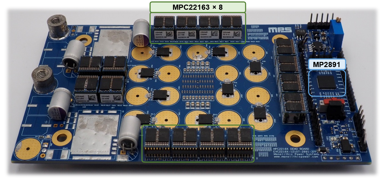
Figure 3: MPS Evaluation Board
PCB Modeling
The complexity of the power and ground polygon shapes and the multi-layer stack-up make it difficult to manually calculate the resistance and inductance from the layout. Instead, the PCB’s scattering parameters (S-parameters) can be extracted using Cadence Sigrity PowerSI, with a 0MHz to 700MHz frequency range. The ports are defined as follows: Port 1 includes the vertical modules on the top side, Port 2 includes the vertical MPC22163-130 modules on the bottom side, Port 3 includes the capacitor connection, and Port 4 includes the connection to load.
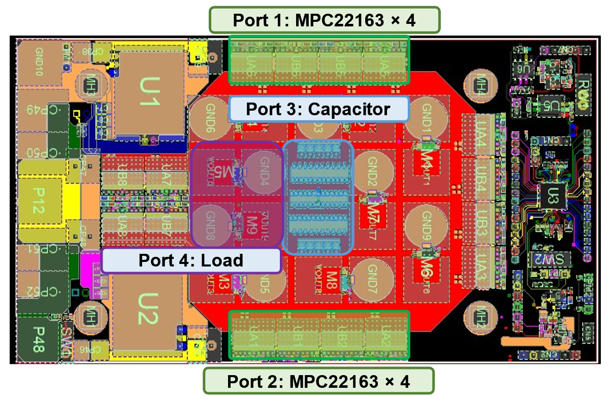
Figure 4: Port Configurations for Extracting the PCB’s S-Parameters
It is important to allocate special ports for the capacitor connections since their effectiveness in mitigating fast transients from the GPU depends on both the quantity and placement. Different capacitor positions affect the PCB’s S-parameters, where ineffective positioning can lead to poor transient mitigation and inefficient power. Generally, it is recommended to place capacitors in a row to minimize differences in path length and to select the capacitance based on the resonant frequency required to meet the target impedance specification.
Two different capacitor types are used in this PDN board design: bulk capacitors and MLCC capacitors. Parameters such as voltage, temperature rating, and construction materials impact the frequency at which the capacitors are effective at filtering. Therefore, to optimize the design, designers must consider the capacitor’s impedance profile using a lumped-capacitance model in the simulations (see Figure 5).
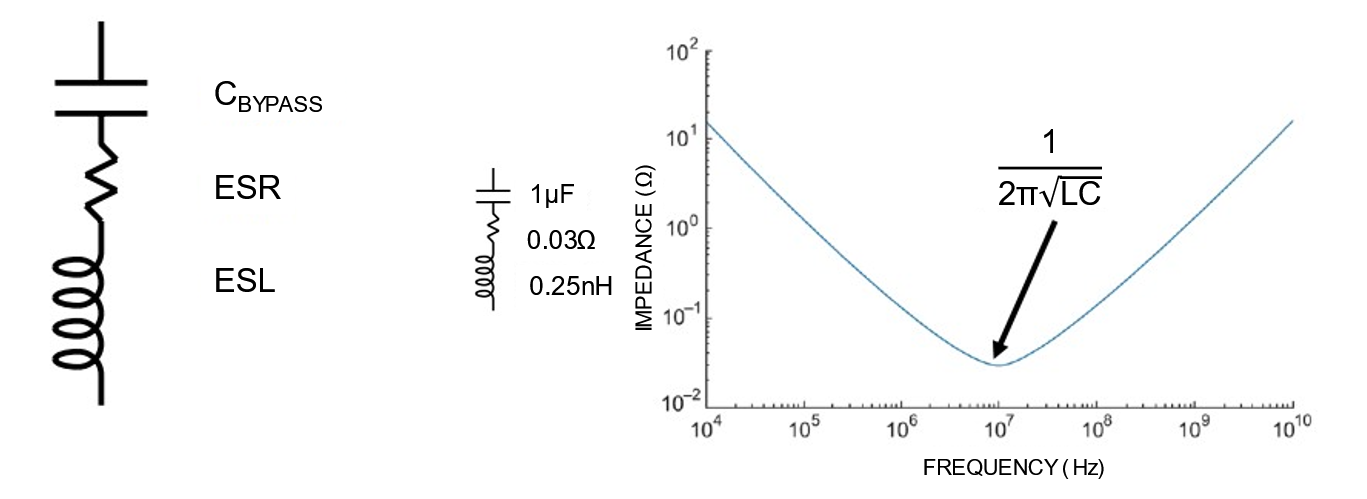
Figure 5: Equivalent Bulk Capacitor Model and Frequency Response
CBYPASS, ESL, and ESR in the lumped-capacitance model define the frequency response of the capacitor’s impedance. The resonance frequency (fO), or the minimum impedance point, can be determined with Equation (1):
$$f_o = \frac{1}{2\pi \sqrt{L \times C}}$$The primary objective of these capacitors is to maintain a low impedance when subjected to high frequencies at which the voltage regulator module (VRM) is inefficient. This inefficiency occurs because the VRM’s effective bandwidth (BW) and phase margin are at low frequencies (<1MHz). Thus, the capacitors must filter out the signals with frequencies outside of the VRM’s BW, typically ranging between a few hundred kHz and a few MHz, which can affect the PDN’s operation.
Figure 6 shows a typical PDN impedance profile that can be divided into three regions: low frequency (0MHz to 1MHz), mid-frequency (1MHz to 100MHz), and high frequency (above 100MHz). This correlation only considers the VRM and the motherboard, which are in the low- to mid-frequency range, and the transient load is applied on the ball grid array (BGA) connector.
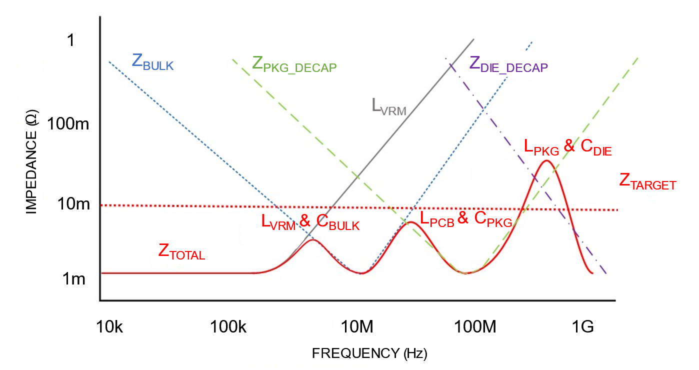
Figure 6: PDN Impedence Profile
Time Domain Simulation
Transient simulation is conducted using the SIMPLIS simulator, a switching power systems circuit simulation software that enables nonlinear features, such as COT control. The MP2891’s SIMPLIS model is combined with the MPC22163-130 and the PCB’s S-parameters that were previously extracted. The S-parameters must be converted to an RLGC model using IdEM from Dassault Systems before being used in the SIMPLIS simulator for transient analysis.
Figure 7 shows the SIMPLIS model of the MP2891 and MPC22163-130, where the S-parameters are added to the schematic as series inductors (L9 and L3) and resistors (R1 and R2).
Figure 7: SIMPLIS Model of the MP2891 and MPC22163-130
Correlation
The SIMPLIS simulation combines the MP2891’s nonlinearity with accurate power delivery modeling to enable accurate prediction of transient behavior on the motherboard. Figure 8 shows a comparison of the SIMPLIS simulation and lab measurement, where the difference is only 5mV.
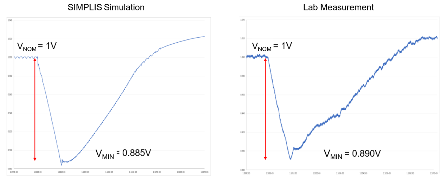
Figure 8: SIMPLIS Simulation vs. Lab Measurement
Conclusion
This article laid out the steps for calculating the inductance required for a buck converter, which includes calculating for duty cycle, turn-on time, ∆IL, L, and IPK. By determining the correct inductance, system efficiency, ∆VOUT, and loop stability can also be optimized.
This article modelled predictive transient simulation using the MP2891, a multi-phase controller, and the MPC22163-130, a two-phase, non-isolated, high-efficiency step-down power block, on an MPS evaluation board. Precise converter models and power delivery network parameters allow for accurate prediction of the multi-phase buck converter’s performance, transient droop, and overshoot. As a result, it is possible to optimize the processor design in the early stages by reducing the number of output capacitors and determining their effective placement. Furthermore, if the design specifications change, accurate simulation enables making a quick assessment of the impact of these changes, as well as identifying any potential issues.
_______________________
Did you find this interesting? Get valuable resources straight to your inbox - sent out once per month!
Technical Forum
 Latest activity 9 hours ago
 1 Comment
Latest activity 2 days ago
1 Comment
Latest activity 3 days ago
4 Comments
1 Comment
Latest activity 2 days ago
1 Comment
Latest activity 3 days ago
4 Comments
Log in to your account
Create New Account