Predicting the VDS Switching Spike with the Parasitic Inductance Effect on SPICE Simulation

Get valuable resources straight to your inbox - sent out once per month
We value your privacy
Introduction
One of the primary goals for the power supply industry is to bring higher power conversion efficiency and power density to power devices in applications such as datacenters and 5G. Integrating a driver circuit and power MOSFET (known as a DrMOS) into an IC increases power density and efficiency when compared to a conventional, discrete MOSFET with an individual driver IC. Moreover, the DrMOS’s flip-chip technology further optimizes the voltage regulator’s performance by reducing response time and reducing the inductance between the die and package (see Figure 1).
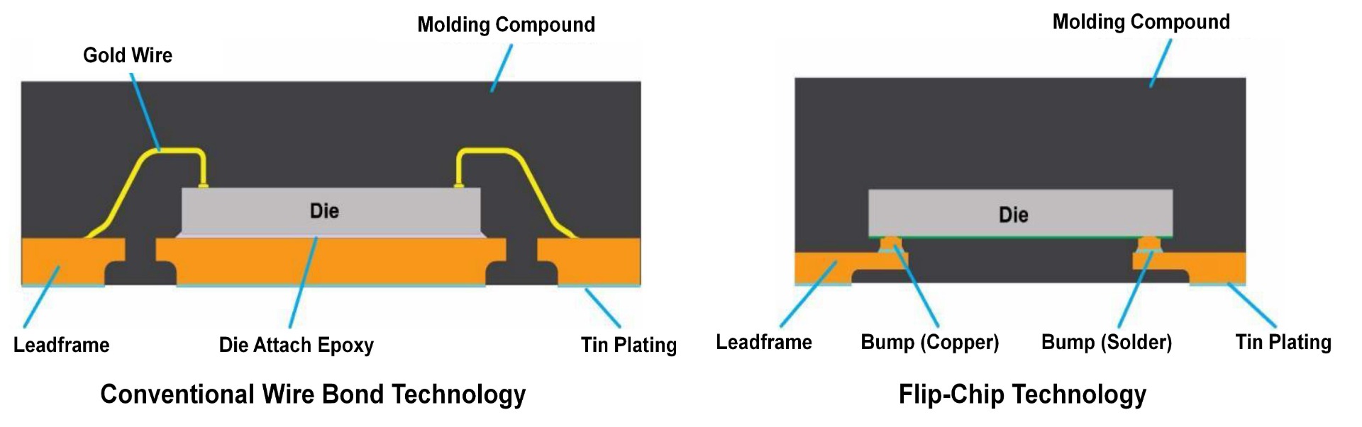
Figure 1: Conventional Wire Bond vs. Flip-Chip Technology
However, parasitic inductance on the substrate and PCB significantly impacts the drain-to-source voltage (VDS) spike, due to the resonant nature between parasitic inductance and the MOSFET’s output capacitance (COSS). A high VDS spike can cause a MOSFET avalanche, which leads to device degradation and reliability issues. To prevent an avalanche breakdown on the MOSFET, there are several methods to alleviate voltage stress.
The first method is to apply a higher-voltage, double-diffused MOSFET (DMOS) process on the DrMOS. If this process is adopted in the power MOSFET design, it results in a higher on resistance (RDS(ON)) for the DrMOS due to a reduced number of paralleled DMOS within the same space.
The second method is to use a snubber circuit to suppress voltage spike. However, this method leads to extra loss on snubber circuit. Furthermore, adding a snubber circuit may not effectively lower the MOSFET’s VDS spike since the stray inductance that causes resonant behavior is mainly integrated in the DrMOS’s package.
When trying to increase voltage regulator efficiency and reduce the MOSFET’s voltage spikes, the tradeoffs described above can make it difficult to quantify and optimize the effects of parasitic inductance on the PCB and substrate. This article will first discuss parasitic inductance modeling. Next, the equivalent parasitic circuit model is applied in a SPICE simulation tool to predict the VDS switching spike. Experimental results will be presented to verify the feasibility of the parasitic model. Lastly, this article will further analyze parasitic inductance optimization on a DrMOS.
Related Content
-
ARTICLE
MPS Power Modules Offer A Compact and Ultra-Low Noise Solution for AMD Xilinx Zynq UltraScale+ RFSoC
The growing number of high-performance FPGA and ASIC applications that are driven by the increased bandwidth of wireless networks and data centers demand for power regulators with high power density, fast load transient response, and high efficiency.
-
VIDEO
Non-Isolated, Two-Phase, Step-Down Intelli-Module for Server Applications: MPC22163-130
The MPC22163-130 is a 130A, non-isolated, two-phase, step-down processor core power intelli-module designed for applications such as AI processors in OAM form factors, FPGA and ASIC core power, and PCIe accelerator cards.
-
APPLICATION

Power Solution for 5G
MPS offers industry-leading power density to meet the demand of these high-power devices.
-
ARTICLE
Analysis and Simulation of PCB ACR Losses for Vcore DrMOS Optimization
Printed circuit board (PCB) main-loop ripple current resistive losses are often neglected and overlooked as a switching power supply loss component.
Parasitic Inductance Modeling on a DrMOS
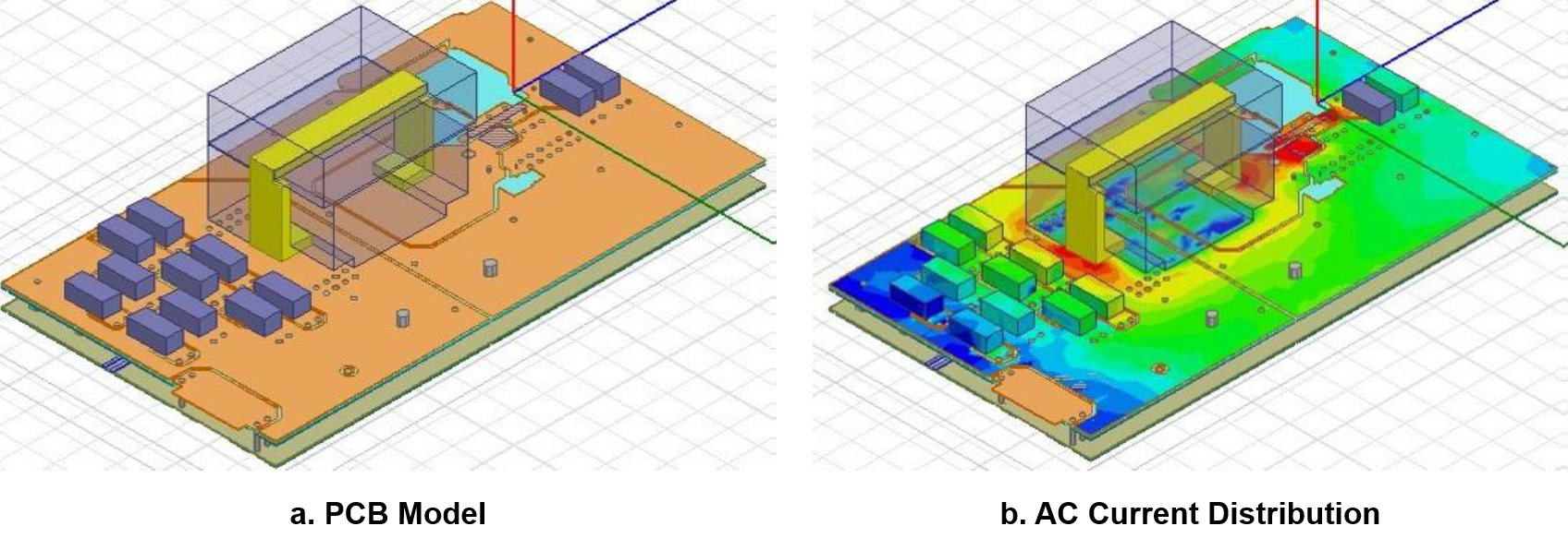
To model parasitic inductance, 3D structures of both the DrMOS and PCB were built for a simulation analysis (see Figure 2). Parameters such as the material, stack-up information, and PCB and package layer thickness are crucial for modeling accuracy.
After 3D-modeling the PCB and DrMOS, the parasitic inductance can be characterized and obtained via ANSYS Q3D. Since this article focuses on the MOSFET’s VDS spike, the main simulation settings of interest are the parasitic parameters on the power nets and driver nets.
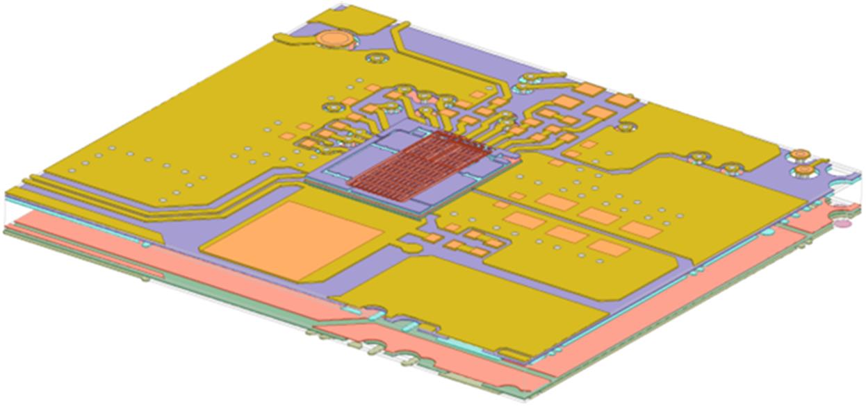
Figure 2: 3D-Modeling Structure of DrMOS and PCB
When considering the parasitic component obtained from Q3D, the parasitic inductance matrix — including the self and mutual terms of each net on the DrMOS — can be selected under different frequency conditions. Since the resonant frequency for VDS on the high-side MOSFET (HS-FET) and low-side MOSFET (LS-FET) is between 300MHz and 500MHz, the parasitic inductance matrix under 300MHz condition is adopted for further behavior model simulation.
Behavior Model Simulation on SPICE
After the equivalent parasitic component model is exported from Q3D, the effects of different types of decoupling capacitors on the PCB are taken into account. Due to the capacitance decay after applying a DC voltage on a multi-layer ceramic capacitor (MLCC), it is important to consider the equivalent circuit of each individual MLCC under certain DC voltage bias conditions. Each consideration should be based on the MLCC’s operating voltage. Figure 3 shows the circuit configuration for the behavior model simulation on SPICE.
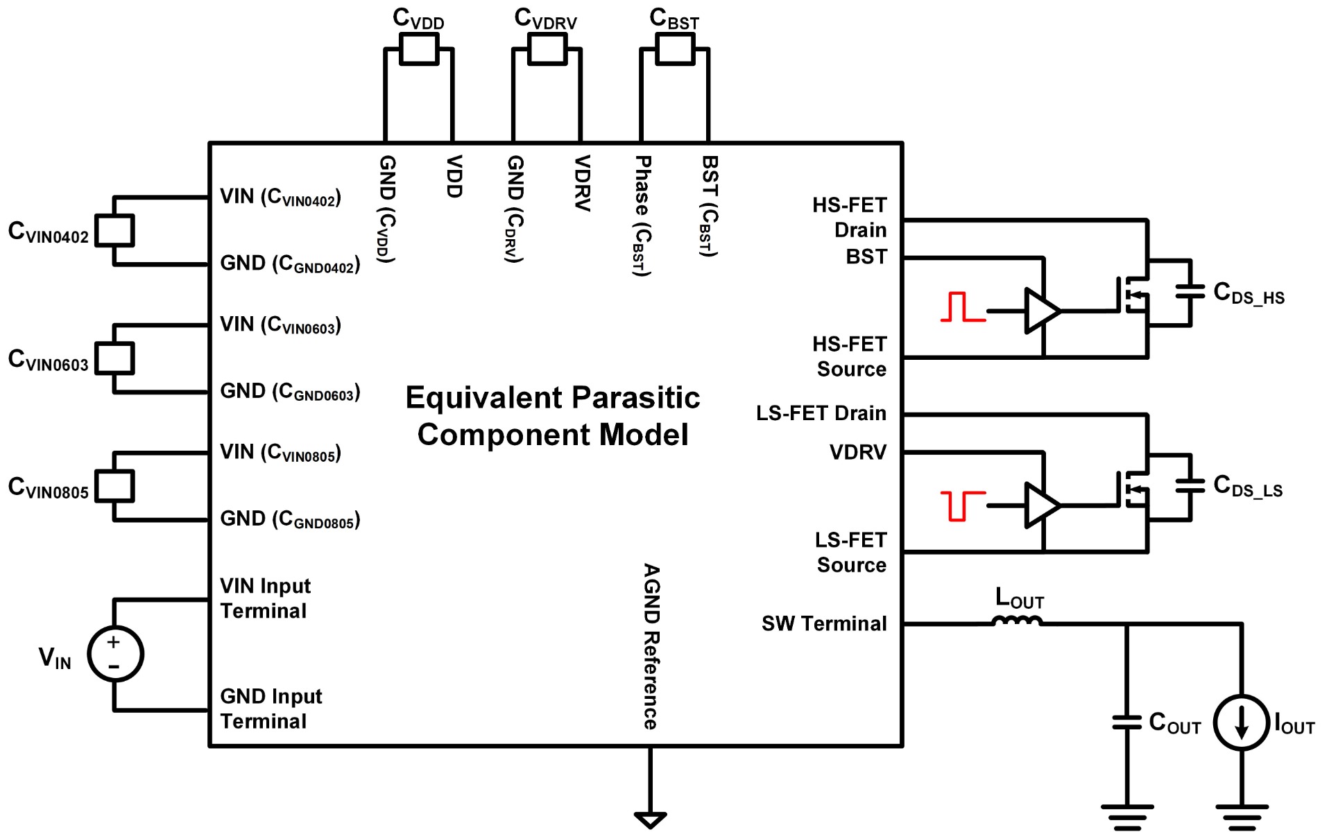
Figure 3: Circuit Configuration of Behavior Model Simulation
Table 1 shows the simulation and measurement conditions based on the schematic shown in Figure 3.
Table 1: Specification on Simulation Scheme and Experimental Test Bench
| Parameters | Value |
| Input voltage (VIN) | 12V |
| Output voltage (VOUT) | 1.8V |
| Switching frequency (fSW) | 800kHz |
| Output inductor | 100nH |
| Load | 50A |
| VDRV / VDD voltage | 3.3V |
DrMOS Solution with the MP87000-L
The MP87000-L is a 90A, monolithic half-bridge with built-in power MOSFETs and gate drivers for server core and graphic card core regulators applications. To suppress voltage ringing, the MP87000-L features Quiet SwitcherTM technology, which is only achievable in monolithic architectures. This technology improves device reliability, lowers EMI, and reduces sensitivity to the PCB layout.
The MP87000-L is ideal for server applications where high efficiency and high power density are required, and it is available in a TLGA-41 (5mmx6mm) package.
Figure 4 uses the MP87000-L to show the simulation and experimental results for VDS on the LS-FET.
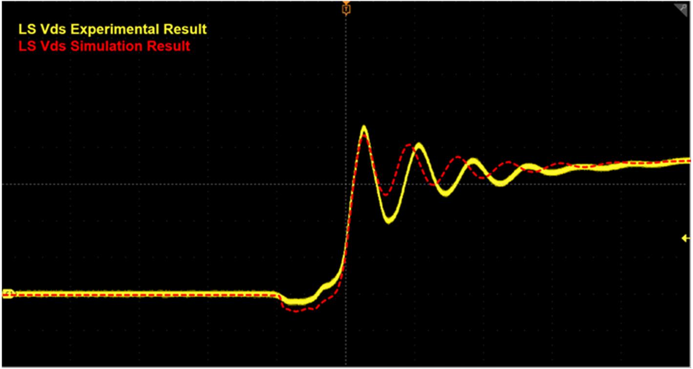
Figure 4: Simulation and Experimental Results for VDS (LS-FET)
Figure 5 uses the MP87000-L to show the simulation and experimental results for VDS on the HS-FET.

Figure 5: Simulation and Experimental Results for VDS (HS-FET)
From Figure 4 and Figure 5, it can be concluded that the VDS spike from the simulation results is almost equal to the experimental results. Table 2 shows additional simulation and experimental results under different load conditions.
Table 2: Simulation and Experimental Results under Different Load Conditions
| Load | Simulated HS-FET VDS Spike | Measured HS-FET VDS Spike | Simulated LS-FET VDS Spike | Measured LS-FET VDS Spike |
| 30A | 14.4V | 15.8V | 12.4V | 13.9V |
| 40A | 14.6V | 15.4V | 12.5V | 13.5V |
| 50A | 17.1V | 16.5V | 13.4V | 13.3V |
| 60A | 19.1V | 19.2V | 12.9V | 13.1V |
| 70A | 21.4V | 21.8V | 13.5V | 13V |
Table 2 indicates that the simulated VDS is congruent with the measured results. In other words, the VDS spike predictions from the behavior model simulation can forecast potential avalanche breakdown on the MOSFET by conducting several optimization approaches that can lower parasitic inductance.
Optimizing Parasitic Inductance
To suppress the VDS spike without compromising efficiency, it is vital to optimize parasitic inductance on the PCB and package. With advanced package technology, input capacitors can be integrated in the package to shorten the decoupling path (see Figure 6). Paralleling the embedded capacitors in the package can effectively reduce the equivalent parasitic inductance on the DrMOS.
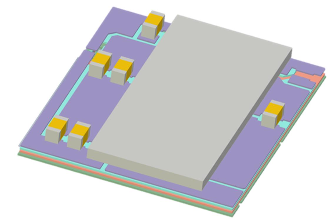
Figure 6: DrMOS Structure with Embedded Capacitors
Table 3 shows the equivalent parasitic inductance and VDS spike when utilizing different decoupling capacitor configurations on the MP87000-L.
Table 3: Equivalent Parasitic Inductance and VDS Spike with Different Capacitor Configurations
| Capacitor Configuration | Equivalent Parasitic Inductance | Simulated HS-FET VDS Spike (Load = 50A) | Simulated LS-FET VDS Spike (Load = 50A) |
| 3 embedded capacitors, 2 PCB 0402 capacitors, 3 PCB 0805 capacitors |
157pH | 17.1V | 13.4V |
| 2 embedded capacitors, 2 PCB 0402 capacitors, 3 PCB 0805 capacitors |
180pH | 18.2V | 14.3V |
| 1 embedded capacitors, 2 PCB 0402 capacitors, 3 PCB 0805 capacitors |
206pH | 21.5V | 16.9V |
| 2 PCB 0402 capacitors, 3 PCB 0805 capacitors |
285pH | 27.7V | 20.6V |
From the simulation results in Table 3, not only is the equivalent parasitic inductance lowered, but the VDS spike on MOSFET is also suppressed. Moreover, thanks to the MLCC’s low-ESR characteristics, no additional power loss is generated on the embedded input capacitors. Therefore, it is possible to add different embedded input capacitors to reduce parasitic inductance in DrMOS applications.
Conclusion
This article discusses the effect of parasitic inductance on the VDS switching spike, as well as several methods to prevent an avalanche breakdown on the MOSFET due to the VDS switching spike.
To quantify the effects of parasitic inductance on the VDS switching spike, parasitic inductance modeling is first introduced, and behavior modeling on SPICE is proposed in this article. The results obtained via SPICE closely matched the experimental results for DrMOS solutions such as the MP87000-L, which means the behavior model can accurately predict the risk of an avalanche breakdown on the MOSFET.
To effectively suppress the VDS spike without any tradeoffs, embedded capacitors in the package were introduced. The behavior model simulation confirmed that these capacitors can reduce the equivalent parasitic inductance, and thus lower the VDS spike without additional loss. MPS offers an extensive portfolio of 48V modules, step-down converters, and processor core power controllers to complete your data center solution.
_______________________
Did you find this interesting? Get valuable resources straight to your inbox - sent out once per month!
Technical Forum
 Latest activity a day ago
 2 Comments
Latest activity 2 days ago
1 Comment
Latest activity 2 days ago
3 Comments
2 Comments
Latest activity 2 days ago
1 Comment
Latest activity 2 days ago
3 Comments
Log in to your account
Create New Account