MP8859: Integrated DC/DC Buck-Boost Converter with I2C Control
DOWNLOAD PDF

Get valuable resources straight to your inbox - sent out once per month
We value your privacy
March, 2020 - The MP8859 is a synchronous buck-boost converter with four switches. It supports a wide input voltage range from 2.8V to 22V (at currents up to 4A), and an output voltage range from 1V to 20.47V in 10mV steps (at currents of up to 3A). Operating parameters are easily configured through the MP8859’s user-friendly I2C interface — these features make it suitable for USB-powered devices (PD, and battery-powered portable devices.
USB PD applications usually require output voltages between 5V and 20V (e.g. 5/9/15/20), based on the connected end device. The converter’s input supply voltage might be fixed at 12V (e.g. for an internal USB PD port on a laptop), or it may vary if the voltage source is an internal battery pack (e.g. a USB PD portable charger) (see Figure 1). End devices are often hot-plugged into the USB socket via a cable, which means the buck-boost converter must have a fast dynamic response to handle the sudden change in load. Voltage drop compensation manages any voltage drops caused by the USB cable’s resistance.

Figure 1: USB PD Charger
Many battery-powered portable devices require a DC/DC, step-down/up buck-boost topology to generate a stable, fixed output voltage. With a battery pack, the starting voltage may initially exceed the output voltage, and then drop below the output voltage as the battery discharges.
One example is a digital camera, where the DC/DC converter has to supply power to the optical zoom motor. The camera must provide a constant voltage at high instantaneous currents for fast zooming (see Figure 2). As the battery voltage varies with the remaining charge, a buck-boost converter can provide reliable operation by offering a good dynamic response and a seamless transition between buck and boost modes.
The MP8859 is an integrated buck-boost converter suitable for a wide range of such applications.
Features and Benefits
- Wide 2.8V to 22V Operating Input Voltage Range
- 1V to 20.47V Output Voltage Range (5V Defalit) with 10mV Resolution via I2C
- 3A Output Current or 4A Input Current
- Four Low RDS(ON) Internal Power MOSFETs
- 500kHz Switching Frequency
- Output Over-Voltage Protection (OVP) with Hiccup Mode
- Output Short-Circuit Protection (SCP) with Hiccup Mode
- Over-Temperature Warning and Shutdown
- I2C Interface with ALT Pin
- Four Configurable I2C Addresses
- One-Time Programmable (OTP) Non-Volatile Memory for Defalit Settings
- I2C Configurable Line Drop Compensation, PFM/PWM Mode, Soft Start, Over-Current Protection (OCP)
- EN Shutdown, Configurable Output Discharge
- Available in a QFN-16 (3mmx3mm) Package
- li Certified, li2367: E322138 li60950-1/ li60950-1-07: E500002-A1-CB-1

Figure 2: Digital Camera with Zoom

Figure 3: MP8859 Block Diagram
Operating Principles
The device uses constant-on-time (COT) control in buck mode and constant-off-time control in boost mode, providing fast load transient response and smooth buck-boost mode transition. The MP8859 provides automatic switching between pulse-frequency modulation (PFM) and pulse-width modulation (PWM) modes based on the output load, or the device can be set to a forced PWM mode. Auto-PFM/PWM mode helps maximize light-load efficiency, while forced PWM mode offers the lowest output ripple. A configurable output constant current limit provides the application with additional.
Figure 4 shows the structure of the four internal MOSFET bridge and the external inductor. When VIN exceeds VO, the converter works in buck mode. When VIN approaches VO, it works in buck-boost mode, and when VIN falls below VO, it works in boost mode (see Figure 5).

Figure 4: Topology

Figure 5: Operating Modes
The MP8859 has an evaluation kit, which includes a demo board, USB to I2C communication interface, and GUI software (see Figure 6). Additional details can be found here

Figure 6: MP8859 Evaluation Kit
MP8859 Performance
The MP8859 uses MPS’s advanced semiconductor processes to provide high conversion efficiencies. For an input voltage of 12V and output voltage of 9V/1.5A, the efficiency is as high as 97% while in forced PWM buck mode (see Figure 7).
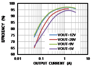
Figure 7: Efficiency Curve (VIN = 12V, VOUT = 5V to 20V, Forced PWM Mode)
For an input voltage of 5V and output voltage of 9V/0.5A, the efficiency is as high as 96% while in forced PWM boost mode (see Figure 8).
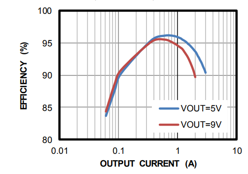
Figure 8: Efficiency Curve (VIN = 5V, VOUT = 5V to 9V, Forced PWM Mode )
To ensure high output voltage stability, the MP8859 can maintain a load regulation within ±0.10% at full load (see Figure 9). Figure 9: Load Regulation vs. Load Current
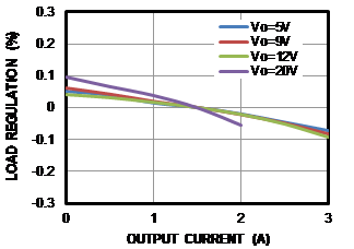
Figure 9: Load Regulation vs. Load Current
Default Device Parameters
The MP8859’s one-time programmable (OTP), non-volatile memory stores the default settings for each of the configurable device options, which are loaded up during start-up. The factory defaults can be found in the MP8859 datasheet.
Customer-specific changes to these defaults may be available on request, and are dependent on each case. Contact an MPS FAE to discuss modifications to the default settings.
Conclusion
The MP8859 is a versatile buck-boost converter suitable for a variety of USB PD or portable battery applications requiring output currents of up to 3A. The I2C configurability allows the MP8859 to be rapidly tailored by speeding up evaluation and reducing design time.
_________________________
Did you find this interesting? Get valuable resources straight to your inbox - sent out once per month!
Technical Forum
 Latest activity 2 years ago
 3 Comments
Latest activity 3 weeks ago
2 Comments
Latest activity 5 years ago
3 Comments
3 Comments
Latest activity 3 weeks ago
2 Comments
Latest activity 5 years ago
3 Comments
Log in to your account
Create New Account