Evaluating the Transient Performance of Buck Regulators with an Integrated Compensation Network

Get valuable resources straight to your inbox - sent out once per month
We value your privacy
Introduction
Designing the compensation network for buck regulators can be tedious and may require several iterations to optimize the solution. Having an optimized control loop, which can enable fast transient response while maintaining proper stability, has become a major challenge with the emergence of new applications such as ADAS and fast transient response requirements. To address these issues, buck regulators with internal compensation networks have been developed to simplify the design process. Despite the benefits of an internal compensation network, there are fewer knobs available to tune/improve the transient performance on the outside. The major challenge is how to evaluate internal compensation networks to ensure that they fit a specific application. This article will provide guidance on how to evaluate internal compensation networks.
Peak Current Mode Buck Regulators
Peak current mode (PCM) control is widely used as the control method for buck regulators. The benefits associated with PCM control over voltage mode (VM) control have already been well established. Figure 1 shows the application schematic and typical bode diagram for a PCM buck regulator.
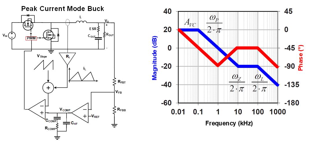
Figure 1: PCM Buck Regulator Schematic and Bode Plot
The two power-stage pole frequencies in Figure 1 can be calculated with Equation (1) and Equation (2), respectively:
$$ω_P \approx {1 \over C_{OUT} \times R_{OUT}} $$ $$ω_P \approx {K_m \times R_i \over L} $$Where Ri can be calculated with Equation (3):
$$R_i=A \times R_s$$And Km can be calculated with Equation (4), when D = 0.5 (D represents the duty cycle):
$$K_m \approx {V_{IN} \over {V_{SLOPE}}}$$The ESR zero frequency in PCM-controlled buck regulators (ωZ) can be calculated with Equation (5):
$$ω_Z \approx {1 \over C_{OUT} \times ESR}$$Typical Type II Compensation Network
Figure 2 shows a typical Type II compensation network. A Type II compensation adds one zero (COMP-Z) and one pole (COMP-P) to a system. The frequency of COMP-Z and COMP-P can be calculated based on the system’s passive components (see Figure 2, Equation (6), and Equation (7)). Note that both the angle/phase and the slope/magnitude due to a pole/zero will start changing at 10% of the pole/zero frequency, and will reach their maximum value at 10 times the frequency of the pole/zero.
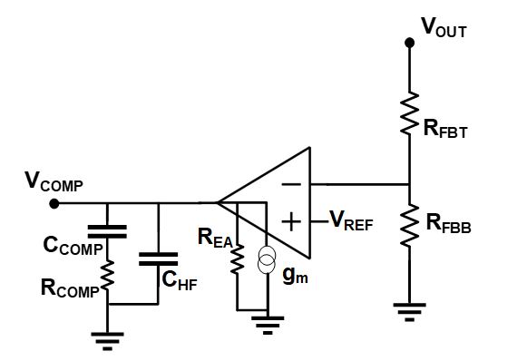
Figure 2: Type II Compensation Network and Zero/Pole Locations
The frequency of COMP-Z can be calculated with Equation (6):
$$ω_{COMP-Z} \approx {1 \over R_{COMP} \times C_{COMP}}$$The frequency of COMP-P can be calculated with Equation (7):
$$ω_{COMP-Z} \approx {1 \over R_{COMP} \times C_{HF}}$$There are two criteria when it comes to the transient performance of buck regulators. One is the system bandwidth (BW), and the second is the system phase margin (PM). The higher the BW, the faster the transient response. The higher the PM, the more stable and quiet the system. Unfortunately, in practice, increasing the BW decreases the PM, and vice versa. This means there is a tradeoff between BW and PM. To have a proper BW along with an acceptable PM and acceptable noise level in a buck regulator, a BW equal to 10% of the switching frequency (fSW) is reasonable.
Guidelines to Evaluate Internal Compensation Networks
Based on the discussion in the previous section, let’s assume that the target BW can be calculated with Equation (8):
$$BW = 0.1 \times f_{SW} $$For a maximum PM, the compensation network zero (COMP-Z) needs to provide its maximum phase boost at the BW frequency. In theory, the positive phase due to a zero reaches its maximum value at 10 times its frequency. Therefore, set COMP-Z between 10% and 20% of the BW frequency. The range accounts for any additional parasitic effects in the system. Therefore, the relation between the COMP-Z frequency and the BW frequency can be calculated with Equation (9):
$$0.1 \times BW < f_{COMP-Z} < 0.2 \times BW $$For proper noise attenuation at higher frequencies, the pole by the compensator (COMP-P) must be approximately equal to fSW / 2, assuming that the switching frequency is 1MHz, then COMP-P must be near the lower value between fSW / 2 and the output capacitor ESR zero, estimated with Equation (5).
An important practical tip to consider is that unless COUT is electrolytic with high ESR, fSW / 2 has a dominant effect, and COMP-P is dependent on that value. This allows COMP-P to be estimated with Equation (10):
$$f_{COMP-P} = {f_{SW} \over 2}$$Since COMP-Z and COMP-P are both defined based on the switching frequency, one can use the two equations to come up with the third requirement, which is the relationship between CCOMP and CHF, and can be calculated with Equation (11):
$$C_{HF} < 4\% \times C_{COMP}$$With these three basic requirements, one can evaluate the performance of the internal compensation networks based on the application’s switching frequency.
Parts with Configurable Switching Frequency
Similar approaches can be applied to parts with configurable switching frequencies, as long as two critical points are considered:
- COMP-Z is set based on the minimum configurable switching frequency.
- COMP-P is set based on the maximum configurable switching frequency.
COMP-Z is set based on the minimum configurable switching frequency because as the switching frequency increases, the inductor size is reduced proportionally. When looking at the second pole in a PCM buck regulator power stage (represented by Equation (2)), the pole frequency (ω_L) increases as the inductance (L) is reduced. As ωL increases, the phase delay caused by this pole is also pushed further out from the BW frequency. The reduction in the negative phase induced by this pole results in an increase in the system’s overall phase, and consequently the system’s PM.
Therefore, if COMP-Z is set based on the minimum configurable switching frequency, the Phase Margin (PM) will increase as the switching frequency increases.
Unlike COMP-Z, the COMP-P frequency is set based on the maximum configurable switching frequency. As discussed earlier, the magnitude/angle due to a pole starts descending at 10% of the frequency of that pole. Let’s assume that fCOMP-P was set based on the minimum switching frequency. Now, if the part was configured to operate at the maximum switching frequency, the phase reduction due to fCOMP-P (which starts taking effect from 0.1 x fCOMP-P) would occur inside its BW. This is not recommended, as it places another pole inside the BW. Since there is only one zero available in a Type II compensation network, it cannot compensate for this pole. Therefore, the COMP-P frequency must be set based on the part’s maximum switching frequency.
Case Study – The MPQ4430
Let’s explore these principles in a real part. The MPQ4330 from MPS is a 36V, 3.5A, synchronous step-down converter with integrated FETs and integrated compensation network. Figure 3 shows the MPQ4430’s typical application schematic and internal compensation network. The switching frequency is set using a resistor at the FREQ pin. Based on the resistor value, the switching frequency of this part can range between 350kHz and 2.5MHz.
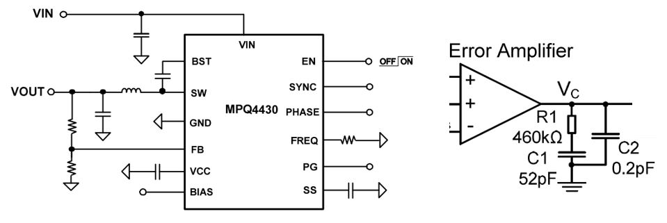
Figure 3: The MPQ4430 Typical Application and Internal Compensation Network
Since the switching frequency is configurable in this part, the approach discussed in the previous section must be followed. COMP-Z must be set based on the minimum switching frequency, which is 350kHz.
Assuming a 350kHz switching frequency, the target BW would be 10% of that, which is 35kHz. Now, let’s calculate the COMP-Z frequency based on the compensation network passive components. In this part, RCOMP and CCOMP are 460kΩ and 52pF, respectively. Using Equation (6), this results in fCOMP-Z being 6.6kHz. This value is within the acceptable range of 4kHz to 8kHz based on Equation (9), which means the first requirement is met.
Next, the COMP-P frequency is checked against the requirement set by Equation (10). Once again, since the switching frequency is configurable in this part, the maximum configurable switching frequency is considered in Equation (10). Considering the maximum switching frequency of 2.5MHz, the target COMP-P frequency (fCOMP-P), must be set close to fSW / 2 = 2.5MHz / 2 = 1.25MHz.
For this part, RCOMP and CHF are 460kΩ and 0.2pF, respectively. This results in fCOMP-P being 1.7MHz, which is close enough to the 1.25MHz target.
Lastly, CHF is compared with CCOMP to ensure the requirement set by Equation (11) is met. In this part, CHF and CCOMP are 0.2pF and 52pF, respectively. Therefore, CHF is approximately 0.3% of CCOMP. So the requirement for the CHF vs. CCOMP value (CHF < 4% x CCOMP) is also met.
MPQ4430 Bode Plot at Different Switching Frequencies
Figure 4 shows the bode measurement of the MPQ4430 as the switching frequency — and consequently the inductor value — both change.
Figure 4: Bode Diagram of MPQ4430 at Three Switching Frequencies

Figure 4: Bode Diagram of MPQ4430 at Three Switching Frequencies
There are a couple of important observations; Table 1 summarizes the results.
Table 1: Summary of Effect of Switching Frequency Increasing on BW/PM
| Switching Frequency | Inductance | Band-Width (BW) | Phase Margin (PM) |
| 350kHz | 8µH | 27kHz | 60° |
| 1.5MHz | 1.8µH | 27kHz | 70º |
| 2.5MHz | 1µH | 27kHz | 77º |
First of all, as seen in the bode measurements, at higher switching frequencies, the PM is improved. This is because, based on Equation (2), the pole due to the inductor (ω_L) is pushed further out as the switching frequency increases. This causes less negative phase at the BW frequency and an increase in the PM, which further confirms that setting the COMP-Z frequency based on the minimum switching frequency is a wise decision.
Note, however, that since RCOMP and CCOMP are fixed, and the increase in the switching frequency only affects the second pole in the power stage, the BW is relatively fixed. Therefore, it may be desirable to increase the BW as the switching frequency increases. This can be accomplished by adding external knobs.
An effective way to increase the loop BW and PM at higher switching frequencies is by adding a feed-forward capacitor (CFF) to the feedback network (see Figure 5).
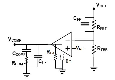
Figure 5: Adding a Feed-Forward Capacitor to the Compensation Network to Improve Transient Response
Adding a feed-forward capacitor can greatly improve the system’s BW and PM. The MPQ4430’s frequency response was taken at a 2.5MHz switching frequency, both with and without a 20pF feed-forward capacitor. With the additional capacitor, BW and PM improved.
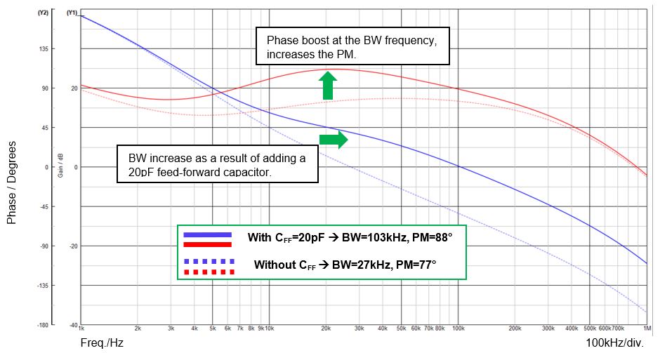
Figure 6: Bode Diagram of MPQ4430 at 2.5MHz With and Without Feed-Forward Capacitor
Conclusion
This article presented a systematic approach to evaluate the capability of the internal compensation networks based on the application switching frequency. The proposed evaluation technique involved three basic checks to ensure that the internal compensation network is properly designed for an application with a known or configurable switching frequency. In certain cases, adding external knobs can further improve the system’s transient performance. These principles were applied to the MPQ4430, which verified the effectiveness of the technique.
_______________________
Did you find this interesting? Get valuable resources straight to your inbox - sent out once per month!
Technical Forum


Log in to your account
Create New Account