Elevating High-Density Adapter Designs with Integrated Capacitive Isolation

Get valuable resources straight to your inbox - sent out once per month
We value your privacy
Introduction
The demand for fast charging has driven the unprecedented evolution of high-density adapters. In practical adapter designs, there are countless implementations of new switching power devices, topologies, and control schemes.
With the introduction of these cutting-edge technologies, the power density of adapter products has significantly increased. 1W/cm3 is becoming the common density for high-density adapters, which is at least two times denser than what was available on the market five years ago. However, as density rises, product designs at the application level are being pushed to their limits. As a result, designers must determine how to exceed the limits of conventional solutions.
The Isolation Requirement
One of the most critical challenges in adapter design comes from the isolation requirement. According to safety regulation standards, an adapter requires reinforced insulation between the primary side’s high-voltage circuitry and the secondary side’s low-voltage circuitry. In traditional solutions, the isolated control is typically implemented by an optocoupler (see Figure 1). This optocoupler only transmits the compensation signal for output regulation under relatively low bandwidth; under these conditions, the optocoupler cannot synchronize the primary MOSFET and the SR MOSFET.

Figure 1: Conventional Flyback Converter Based on Optocoupler
As a result, SR control in conventional schemes can be only implemented by monitoring the secondary-side winding voltage. Because the SR MOSFET can only turn off after the primary MOSFET turns on, there is always shoot-through during continuous conduction mode (CCM). If the SR MOSFET does not turn off quickly enough, the extended shoot-through can result in a large reverse current and a high voltage spike. These high stresses can cause critical reliability issues. To avoid these issues, it is recommended to implement layout restrictions and use a large snubber. However, the increased component size and power consumption of these additions further limit power density.
Solution for Capacitive Isolation
The MPX2002 and MPX2003 are effective, all-in-one solutions that integrate capacitive isolation into a flyback and SR combo controller. Figure 2 shows that the integrated pair of high-voltage capacitors can withstand 4500VRMS for 60s. This allows the isolation withstand voltage rating to meet the reinforced isolation requirement for most safety regulations. In addition, a high-speed communication channel is established across the high-voltage capacitors. This channel enables the design to achieve reliable, accurate synchronization between the SR and the primary-side switching.

Figure 2: Flyback Converter Based on the MPX2002 or MPX2003
Figure 3 shows that a typical 30ns dead time between the SR gate and the primary flyback gate is guaranteed under all operating conditions by the IC’s internal logic. This significantly reduces the shoot-through risk during CCM, which eliminates the need for an oversized snubber that could handle the high-voltage stress caused by shoot-through.

Figure 3: Typical Waveforms for the SR Gate and Primary Gate in MPX2002 Solutions
In addition to the synchronization signal, the communication across the MPX2002 and MPX2003’s isolation capacitors also carries the output regulation signal via pulse-frequency modulation (PFM). During PFM, the switching frequency (fSW) and the flyback converter’s peak current are controlled by the PFM signal, which means that the solution does not require an optocoupler. Note that the MPX2002 and MPX2003 are respectively optimized for a rated fSW of 65kHz and 130kHz. As a result, optocouplers are no longer necessary when solutions are built based on the MPX2002 and MPX2003.
Eliminating the need for additional components addresses another critical challenge for high-density adapters: small layout space. Fast-charge adapters require higher power and more functions, which means more components are being squeezed into a smaller space. By simplifying the overall solution, features such as reduced component count can be crucial for space-constrained applications.
Figure 4 shows a 40mmx40mmx25mm 65W PD adapter designed based on the MPX2003. Without an adapter case, the power density can be as high as 1.63W/cm3. Even when all the components required to implement the PD protocol are added on the secondary side, there is still additional layout space.
Solutions with integrated capacitive isolation provide an additional benefit, as the IC can be placed directly beneath the transformer. Conventional solutions typically place all components (except for the optocoupler) far from the transformer due to the clearance requirement of safety regulations. This feature reduces the PCB layout size.
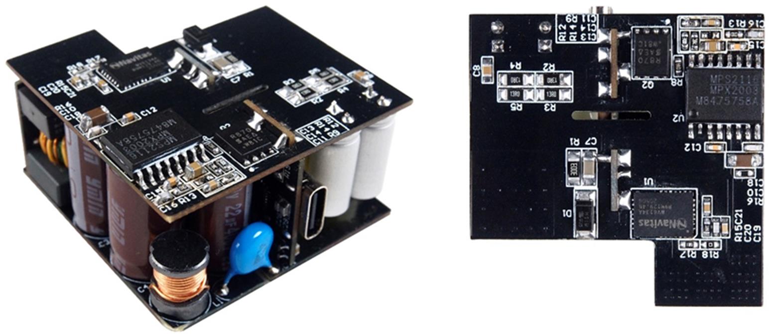
Figure 4: 65W PD Adapter Design Based on the MPX2003
Highly integrated flyback controllers significantly improve efficiency and power density in several ways:
- The SR’s accurate timing control eliminates the need for an oversized snubber, which benefits space-constrained applications
- An advanced CCM and quasi-resonant (QR) hybrid control scheme ensures optimized operating states for a wide operating range
- A significantly reduced component count reduces BOM and time-to-market
- Effectively utilizing the space beneath the transformer also reduces PCB size
Figure 5 shows that the efficiency can pass the mainstream energy regulation thresholds with a large margin for any output voltage (VOUT) required by the PD protocol. Under full loads, the efficiency remains high, which simplifies thermal design.
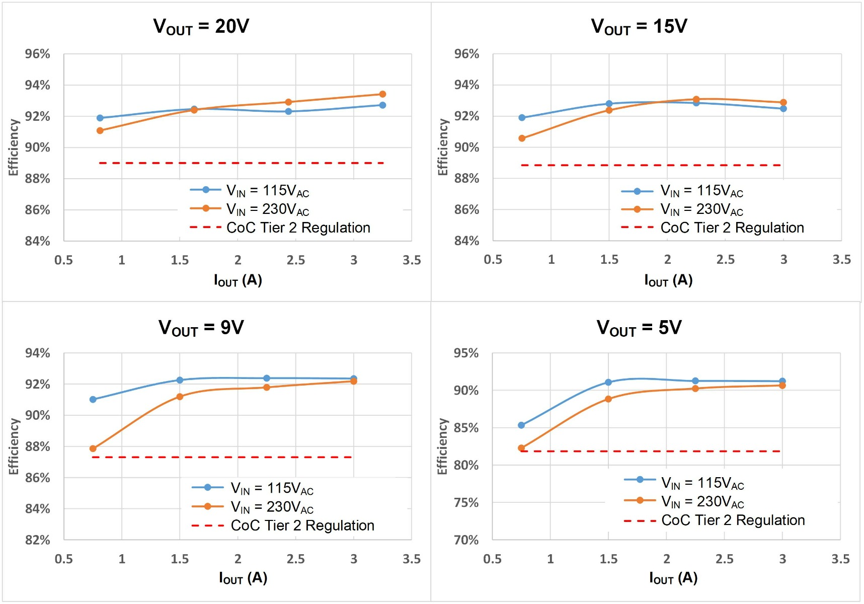
Figure 5: MPX2003 Efficiency (65W PD Adapter Design)
Conclusion
The integration of capacitive isolation surpasses the expectations for traditional solutions that use optocouplers. In particular, flyback controllers such as the MPX2002 and MPX2003 demonstrate the effectiveness of integrated solutions with their tiny size, high efficiency, and layout flexibility.
Overall, integration provides multiple benefits, such as more accurate synchronization between the SR and primary-side switching, reduced component count, and a more compact layout. In addition, these solutions enable the implementation of a more advanced control scheme to further improve efficiency and power density, which will pave the way for future high-power density adapters.
_______________________
Did you find this interesting? Get valuable resources straight to your inbox - sent out once per month!
Technical Forum
 Latest activity a month ago
 2 Comments
Latest activity 2 months ago
2 Comments
Latest activity 2 months ago
2 Comments
2 Comments
Latest activity 2 months ago
2 Comments
Latest activity 2 months ago
2 Comments
Log in to your account
Create New Account