Digital Communication in Power Supply Applications

Get valuable resources straight to your inbox - sent out once per month
We value your privacy
Despite the increasing popularity of digital interfaces, it is not widely understood how a power subsystem’s digital interface can benefit a specific electronic application. This article summarizes the aspects of common physical interfaces and protocols available today, using MPS digital power solutions as examples for a variety of applications.
Digital communication and control benefit power converter subsystems and the systems they are part of. A digital interface provides the power design engineer with greater flexibility to finalize and optimize certain parameters (e.g. sequencing of voltage rails, fault protection thresholds, and feedback compensation) after a system board returns from assembly.
Using the OSI model for digital communication, there are two major aspects of digital communication: the physical layer (PHY) over which communication is executed, and the protocol or a command set that is used to communicate information.
- The physical layer (PHY) for most power converters is the I2C serial interface, or its derivative SMBus . It allows multiple converter circuits to share a single interface with a host controller, and is used in multiple subsystems in servers and PCs .
- The data link layer defines the information to be communicated between the host and voltage converter circuit. The data can be defined as a set of addressable registers with data bits uniquely defined for each IC, or the registers can follow an industry standard.
(For the distinction between I2C, SMBus, and PMBus, refer to the PMBus website.)

Figure 1: I2C/PMBus Signals
The I2C interface defines a bidirectional clock signal (SCL) and a bidirectional data signal (SDA). PMBus adds the alert signal to this, along with a defined set of registers/commands to communicate status. Signal timing for clock and data are the same for both standards.
The PMBus standard states that to be considered compliant with the specification, a power device must implement at least one of the PMBus commands. Most PMBus-equipped devices implement the PMBus protocol for common commands, such as setting the output voltage or reading die temperature. However, nearly all devices also implement MFG_SPECIFIC registers unique to that device. In addition, the PMBus standard calls out two methods to encode values into a digital word that can be communicated over the interface: direct and linear. For the direct method, the value in the command is the integer value defined for the register in the device.
Linear Data Format
Linear data format is a form of floating-point value representation. In practice, most devices use either a Linear11 or Linear16 representation of data values.
Linear11 Data Format
This data format has an 11-bit mantissa and a 5-bit exponent (see Figure 2). Both the mantissa and the exponent are two’s complement integers, meaning they can be positive or negative.
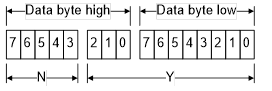
Figure 2:Linear11 Data Format
Convert a real-world value to Linear11 format with Equation (1):
XREAL WORLD=Y∙2N
N can be positive or negative, and 2N defines the size of an LSB of the Y mantissa. The smallest number that can be represented using Linear11 format is ±2-16 x 1 = ±15.3e-6. The largest number is ±33.5e6.
Since a signed, 11-bit integer goes from -1,024 to +1,023, the magnitude of the mantissa should be between 512 and 1,023. This points a way to encode a real-world value as a PMBus Linear11 formatted value. Start with N = -16, then increment N until the magnitude of the mantissa is within the desired range.
Linear16 Data Format
Linear16 format is similar to Linear11, except that the full 16-bit I2C command packet is used for the mantissa and the exponent is supplied separately (see Figure 3). For example, the MPQ4230 buck-boost converter from MPS uses this format for VOUT_COMMAND and READ_VOUT, which set and read the output voltage.
This data format has a 16-bit mantissa and a 5-bit exponent. Both the mantissa and the exponent are two’s complement integers, meaning they can be positive or negative.
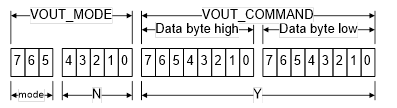
Figure 3: Linear16 Data Format
Convert a real-world value to Linear16 format with Equation (2):
Xreal world=Y∙2N
With a 5-bit exponent, the smallest number that can be represented using Linear16 format is still ±2-16 x 1 = ±15.3e-6. However, the target value for the mantissa is now between 214 and 215, or between 16,384 and 32,767. This gives more resolution with which to set and read the output voltage. Table 1 shows the VOUT_MODE command definition.
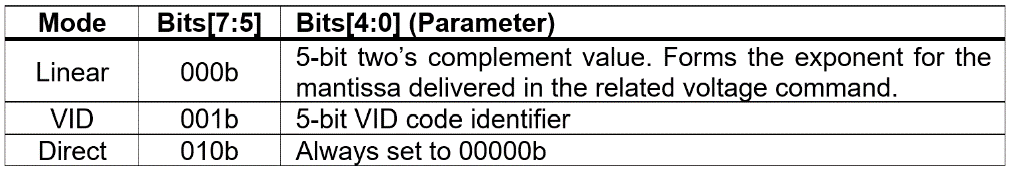
Table 1: VOUT_MODE Command
Typical PMBus Commands
PMBus commands can set the output voltage of a converter, enable the device, determine whether a warning threshold has been exceeded, and report a fault. >Underlying faults can be reset with a command, such as the STATUS_WORD command for MPS’s MPM3695-25 power module (see Table 2).
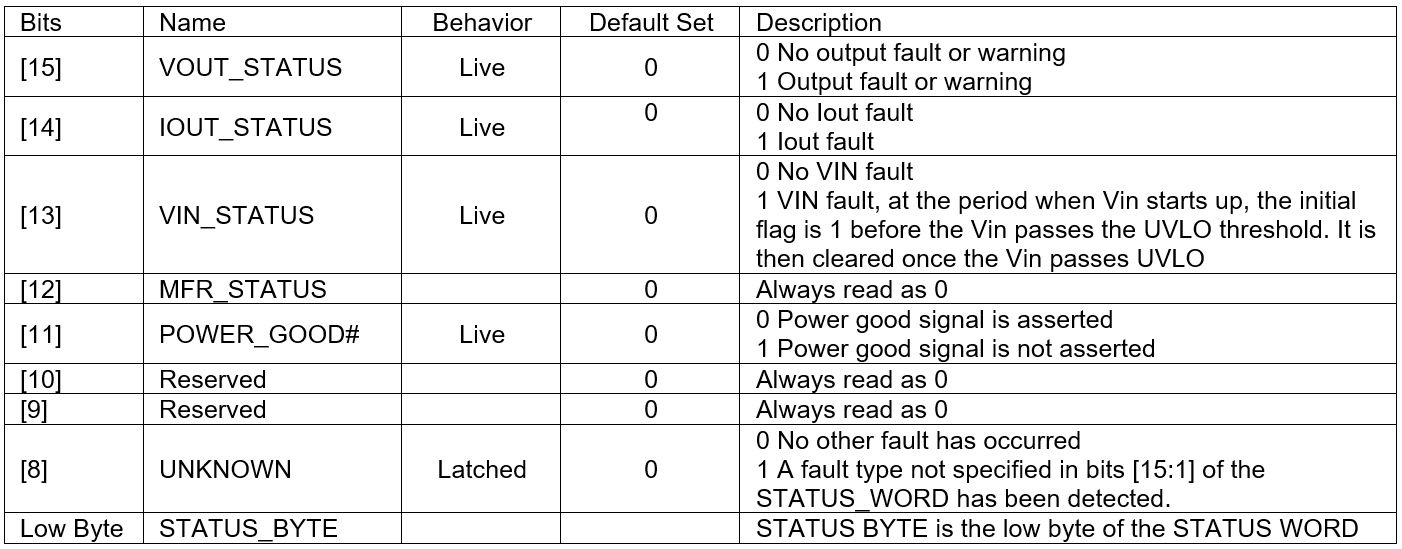
Table 2: Status Word (Addr/Command 0x79)
Manufacturing-specific commands are unique to a given device. Consider the MPM3695-25’s MFR_CTRL_COMP command. While STATUS_WORD is a common command for many ICs, the constant-on-time compensation loop for the MPM3695-25 is unique to this chip. Table 3 lists the MFR_CTRL_COMP bit definition.
Table 3: MRF_CTRL_COMP (Addr/Command 0xD0)
Memory Options for Converters with a Digital Interface
Converters that can communicate over a digital bus also differ in terms of available memory options. There are three memory classifications:
- No permanent memory in the converter: In this case, the configuration is stored in the memory of the host microcontroller (µC), and the converter configuration must be loaded after every start-up. This can simplify the design and lower costs, but requires a means to power the host µC at start-up. To boot the converter, the system requires either a separate bias converter for the µC, or the default registers in the digital converter must be sufficiently close to the configured values. The MP8843 is a synchronous buck converter with an I2C interface that must be reconfigured after each start-up. This device is ideal for applications requiring fine adjustment of the core voltage for a µC core in a system-on-chip (SoC), or similar digital ASIC. These application systems contain firmware in flash memory, which can write to the device’s I2C interface to adjust the core voltage, and to optimize processor speed and power dissipation. For example, the MP8843 has some unique registers, and minimizes cost by eliminating the overhead requirement for the PMBus.
- One-time-programmable (OTP) memory: OTP is a cost-effective, reliable solution for high-volume products. However, it requires the IC supplier to create a unique part number for each application. The MP8859 from MPS is an example of a 4-switch buck-boost converter with an I2C interface and OTP memory. It can set the output voltage, max current, switching frequency, and fault recovery behavior. A graphic user interface (GUI) program is provided to select the register values that optimize the user’s application. When the complete set of register values is determined, they can be permanently stored using the GUI. After the OTP is written, the stored values become the default start-up values for the registers. The application can still change the registers through the I2C interface after start-up. Once register values have been determined during end-product development, those values are written into the converter OTP memory at manufacturing time. MPS writes these values when the IC is tested at the semiconductor factory, eliminating this manufacturing step for the user.
- Non-volatile memory (NVM): NVM provides the highest flexibility, but at a higher cost. Users must be aware of the type of the memory used to implement NVM. Flash memory is widely used in µCs, but can degrade quickly when operating at high temperatures, which is often a concern for power converters. For this reason, companies such as MPS do not utilize flash memory in its products.
The MPQ8645P is a 30A, parallelable, point-of-load (POL) converter for telecom and server applications. Its registers conform to PMBus standards, and the register values can be saved to the NVM multiple times. This means the hardware can be repeatedly prepped and tested as if it were being assembled/manufactured as new hardware. In these cases, users should store configuration information during product development exactly as they would during volume manufacturing.
Converter ICs with no permanent memory often do not follow PMBus standards for register definitions, which minimizes overhead for these configuration registers. With just a few optimized registers, the effort to develop firmware to read and write to these registers is manageable. However, developing the firmware to interface to a device with dozens of configuration and monitoring registers can be daunting, so making the register definition follow PMBus standards can be very valuable.
Conclusion
Adding a digital control and communication feature to the power converter allows better integration of these devices into modern electronic systems by streamlining system design, and increasing flexibility and reliability. However, the best way to reap the benefits of these features is for a design engineer to familiarize themselves with different approaches to converter designs with the digital interface and control, as well as the specific nomenclature of these devices.
Log in to your account
Create New Account