Designing an Active-Clamp Forward Converter for PoE-bt Applications (Part II)

Get valuable resources straight to your inbox - sent out once per month
We value your privacy
Introduction
This article is the second part of a two-part series exploring how to design an active-clamp forward controller for PoE-bt applications. Part I covered PoE applications, as well as the basics for forward converter topologies and active clamps. Part II will review secondary-side synchronous rectification MOSFETs, secondary spike absorption circuits, and efficiency verification processes for PoE-bt applications.
Synchronous Rectification
The secondary side of the forward circuit typically requires two freewheeling diodes for the excitation inductance and the output inductance. These diodes lead to considerable losses during the freewheeling process under high-current outputs. Therefore, MOSFET transistors are often used instead of diodes to improve efficiency. The forward converter’s primary-side main switch corresponds to the freewheeling process of the magnetizing inductance and the output inductor. As a result, the switching voltage of the secondary-side transformer can drive the secondary-side synchronous rectification (SR) MOSFET.
The freewheeling MOSFET has a gate-to-source voltage (VGS) that is rectified by the SR MOSFET’s drain-to-source voltage (VDS). When the magnetizing inductance and the output inductor current are both low, the output voltage turns on the rectifier MOSFET through the transformer. The secondary side then works in forced continuous conduction mode (FCCM), leading to a higher no-load loss than a traditional diode rectification topology.
When the output voltage is high, the triode voltage regulator circuit protects the secondary-side MOSFET’s VGS from reaching a high voltage (see Figure 1). Meanwhile, for the MOSFET gate that is connected to the emitter, the driving voltage follows any changes in the transistor’s base voltage. The transistor’s collector terminal can then take power from the transformer or the output voltage.

Figure 1: Triode Voltage Regulator Circuit
The MOSFET transistor drive circuit leads to additional losses. The larger the difference between the output voltage and the clamping voltage driven by the MOSFET transistor, the greater the drive circuit loss. This makes forward topology well-suited for applications with low voltages and high currents.
Secondary Spike Absorption Circuit
When the secondary-side rectifier MOSFET (QR) shuts down and the secondary freewheeling MOSFET (QF) opens, there may be transformer leakage inductance. The leakage inductance then affects the QR drain-to-source capacitance (CDS), and ringing is superimposed on VDS. Higher spikes affect the forward converter’s efficiency. A conventional RC absorption circuit can suppress VDS ringing on QR, though it also leads to a relatively large power loss.
An RCD absorption circuit is recommended to reduce power loss (see Figure 8). When QR starts up, the leakage inductance energy can be stored in a capacitor (C) through a diode (D). When QR shuts down, the energy stored in the capacitor can be transferred to the output capacitor and the load through the resistor (R). A larger-value capacitor results in a smaller ringing amplitude. Meanwhile, a larger-value resistor reduces the power loss and ringing amplitude.

Figure 8: RCD Absorption Circuit
Figure 9 shows how the ringing peak drops by 20% with the addition of a Schottky diode (D). In this scenario, the capacitance (C) can be set to 2.2nF, and the resistance (R) can be set to 20kΩ.
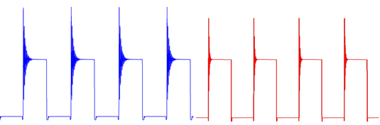
Figure 9: Ringing Periods Before and After Implementing a Schottky Diode
Efficiency Verification
To verify the forward converter design, forward and flyback topologies at different power levels with an output voltage of 5V/3.3V were compared. In active-clamp forward topology, the auxiliary switch can work with zero voltage switching (ZVS) due to the delay time between when the main switch starts up and the auxiliary switch starts up. It should be noted that ZVS can become complicated with the main switch.
Before switching, the auxiliary switch and the rectifying MOSFET are open. When the auxiliary switch turns off, the following occurs:
- The current flowing through the main switch drops
- The rectifying MOSFET’s voltage drops
- The freewheeling MOSFET’s voltage drops
- The DS capacitance drops
- The main switch’s VDS starts to drops
The inductor current can still flow through the body diode of the rectifier MOSFET, which clamps the voltage across the transformer at a lower voltage amplitude and prevents the main switch’s VDS from falling further. When the main MOSFET turns on, its VDS is almost equal to the input voltage, which can lead to start-up losses.
By calculating and analyzing the power loss when the output is 3.3V/50W, the auxiliary switch detects ZVS and the smaller excitation current, so the power loss is small. The main switch’s loss mainly consists of partial start-up loss and conduction loss. The transformer loss consists of magnetic loss and copper loss. The secondary-side rectifier MOSFET’s loss consists of switching loss, conduction loss, and diode loss caused by oscillation. The output inductor loss consists of magnetic loss and copper loss.
Figure 10 shows the prototype efficiency curve. As the output power increases, the forward converter’s efficiency is typically better than that of the flyback converter at higher output power levels due to the improved thermal management in PoE applications.
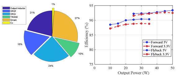
Figure 10: Efficiency Curve
Conclusion
In this article, we reviewed how MOSFET transistors and RCD absorption circuits can improve efficiency for active-clamp forward converters, then verified these theories. Overall, PoE solutions using active-clamp forward converters provide higher efficiency and overcome the shortcomings of RCD clamp circuits, further enhancing the function of PoE-bt applications.
_______________________
Did you find this interesting? Get valuable resources straight to your inbox - sent out once per month!
Technical Forum
 Latest activity a month ago
 2 Comments
Latest activity 2 months ago
2 Comments
Latest activity 2 months ago
2 Comments
2 Comments
Latest activity 2 months ago
2 Comments
Latest activity 2 months ago
2 Comments
Log in to your account
Create New Account