Controlling Primary-Side Ringing

Get valuable resources straight to your inbox - sent out once per month
We value your privacy
Introduction
The flyback power supply is one of the most commonly used topologies. Typically, the transformer’s leakage inductance causes primary-side ringing, which generates voltage spikes that damage the MOSFET. It is essential to design the transformer and MOSFET components to control ringing. MPS has introduced an RCD clamp circuit design strategy to reduce leakage inductance. This circuit is described in further detail below.
RCD Clamp Circuit Design
In flyback circuits, the transformer transfers the primary-side energy to the secondary side once the MOSFET tube turns off. However, the leakage inductance energy cannot be transferred. This causes ringing on the stray capacitor in the circuit. While the leakage inductance is the root cause of the ringing, it cannot be fully eliminated, and is between 1% and 5% of the overall inductance. Instead, the leakage inductance can only be reduced with the winding method.
Figure 1 shows the sandwich winding method, a conventional approach used to reduce leakage inductance. Similar to the process of making sandwiches, the primary winding (NP) is divided into two, then the secondary winding (NS) is wrapped around half of NP, the auxiliary winding, and the remaining half of NP.

Figure 1: Sandwich Winding Method to Reduce Leakage Inductance
Figure 2 shows the inversion circuit after the MOSFET turns off, when the voltage at both ends is composed of three parts: the maximum input voltage (VINMAX), the secondary refracted voltage (VOR = n x VO), and the peak voltage (VSPIKE) generated by the ringing. When the ratio (n) and MOSFET are selected for the input and output voltage, VSPIKE must be suppressed as much as possible to ensure that the MOSFET operates within the stress range. To suppress ringing, engineers typically select an RCD clamp circuit because of its simple design, low cost, and ability to effectively suppress voltage spikes.
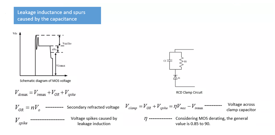
Figure 2: Suppression of Peak Voltage to Ensure MOS Operates Within Stress Range
Correctly selecting the RCD clamp circuit is crucial because suboptimal resistor and capacitor values increase MOSFET stress or circuit power consumption. Figure 3 shows that when MOSFET turns on, energy is stored in the magnetizing inductance (LM) and the leakage inductance (LS). When the MOSFET turns off, the energy in LM transfers to the secondary side, but the leakage inductance energy remains. Then the leakage inductance is released to turn on D1, which charges C1. Once the charging voltage reaches VCLAMP, D1 turns off and C1 discharges through R1.

Figure 3: Energy Transfer when the MOSFET Turns On/Off
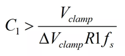
R1 must be derated by 1/3 of the resistance power during selection. According to the principle of energy conservation, R1 can be calculated with Equation (1):
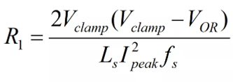
The clamping capacitance (C1) should be large enough to achieve a low, pulsating voltage while absorbing the leakage inductance energy. The pulsating voltage is typically calculated to be within 5% to 10% of the clamping voltage. To determine the minimum value for C1, choose the smaller parasitic between R and L. This minimum C1 can be calculated using Equation (2):
MPS Solution
MPS provides an exceptional selection of power solutions to optimize primary-side regulation (PSR). The MPX2002 is an all-in-one flyback controller that features an integrated primary driving circuit, secondary controller, synchronous rectification driver, and safety compliance feedback. The device’s synchronous rectifier (SR) can safely operate in continuous conduction mode (CCM) by matching the primary-side MOSFET’s driving signal. The MPX2002 does not require auxiliary winding to drive the low-side SR MOSFET, even when the output is insufficient. This improves on the conventional sandwich winding method from Figure 1.
The MP8017 is an IEEE 802.3af-compatible, power-over-Ethernet (PoE) powered device (PD). It is specifically designed for active-clamp PSR in a flyback topology. The device can also be set to secondary-side regulation (SSR) for active-clamp flyback topology by placing an optocoupler on the secondary side.
Conclusion
In conclusion, RCD circuit design can be used as a simple and effective suppression method to control flyback primary-side ringing. By carefully selecting the resistor and capacitor, the clamp circuit can better absorb the leakage inductance energy. In addition, the RCD clamp circuit does not consume the main excitation inductance capacity, and reduces both the peak voltage and the power device’s switching stress.
To learn more about RCD circuit designs, read our Part I and Part II series on designing an active-clamp forward converter.
_______________________
Did you find this interesting? Get valuable resources straight to your inbox - sent out once per month!
Technical Forum
 Latest activity a month ago
 2 Comments
Latest activity 2 months ago
2 Comments
Latest activity 2 months ago
2 Comments
2 Comments
Latest activity 2 months ago
2 Comments
Latest activity 2 months ago
2 Comments
Log in to your account
Create New Account