Controlling Excessive Conducted EMI Under a Long-Line Load (Part III)

Get valuable resources straight to your inbox - sent out once per month
We value your privacy
Introduction
This article is the final part of a three-part series exploring methods for analyzing and improving excessive EMI under long-line loads. Part I discussed the common-mode (CM) EMI model and considered the influence of electric field coupling and magnetic field coupling. Part II validated the transmission line theory through a series of computations. Part III will focus on three methods that were implemented to reduce noise.
Noise Reduction Methods
Based on the noise model, there are multiple ways to reduce noise, described below:
- Reduce the high-frequency noise sources (i.e. reducing the switching waveform’s slope)
- Reduce high-frequency noise using frequency jittering
- When wiring, minimize the area of the dV/dt node and the dI/dt loop
- Add a common-mode (CM) filter to the loop, or add a snap-on ferrite filter (also called a magnetic ring) to the output line
- Alter the output line length to avoid sensitive frequency bands
- Add a shield to mitigate issues caused by near-field coupling
Consider these general methods. The final three methods discussed above focus on long-load lines. These methods will be examined further in this article.
Adding a Snap-On Ferrite Filter
To implement the first noise reduction method, add a snap-on ferrite filter on the output side (at one end close to the board). Figure 1 shows a comparison between the output line to ground impedance with and without a snap-on ferrite filter. When the snap-on ferrite filter is added, the impedance to the ground significantly increases, which can mitigate the effects of resonance.
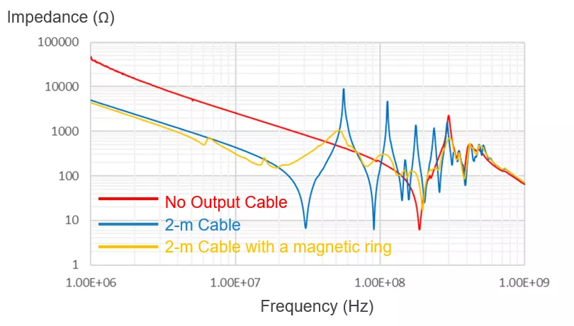
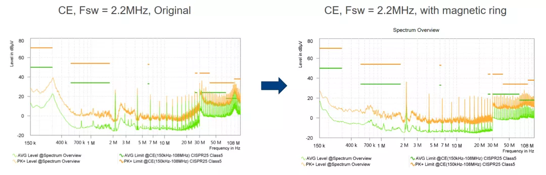
Figure 2 shows the output line’s conducted EMI. When a snap-on ferrite filter is added, it effectively suppresses the high-frequency resonant peak.
Adjusting the Output Line Length
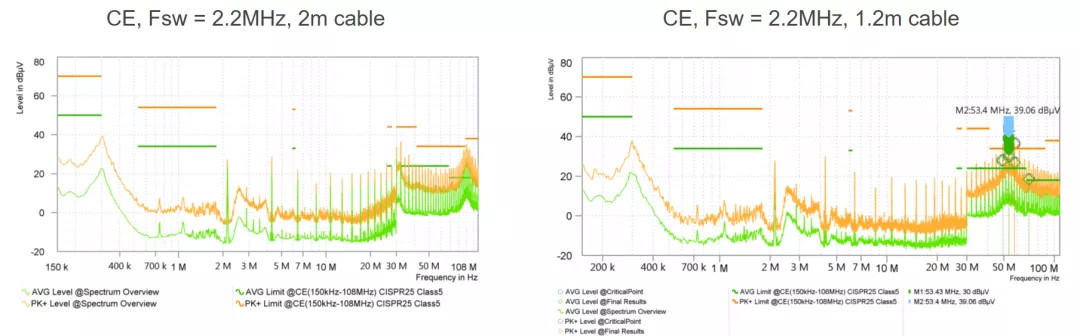
For the second noise reduction method, change the output line length to adjust the resonant peak’s position. Figure 3 shows that when the line length is 1.2m, the resonant peak corresponding to 3/4λ exceeds 108MHz, avoiding the FM band (76MHz to 108MHz). Therefore, changing the line length can reduce noise. When comparing the 2m and 1.2m line lengths and their respective conducted EMI results, the latter line’s resonant peak occurs at about 53MHz.
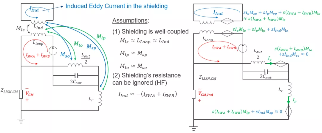
Adding a Shield
It is possible to add a shield that reduces EMI by eliminating the near-field coupling between the output line and the test board. The shield can be made of metal. Wrap the dV/dt node and dI/dt loop in the circuit, then ground the shield close to the noise source.
Figure 4 shows how grounding effects electric field coupling. When the dV/dt node is shielded, the stray capacitors (CSWP and CCOU) that were originally directed to the reference-to-output line act as stray capacitors (CSWP1 and CCOU1) to the shield. When the shield is grounded, the noise current directly flows back to the noise source’s ground without passing through LISN, resulting in no CM noise.
If the shield is not grounded, the noise current still flows to the reference ground, though this does not reduce EMI. This is because the shielding case retains stray capacitance from the reference ground and the output line.
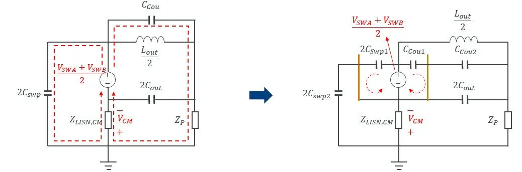
Figure 5 shows the effects of grounding on high-frequency magnetic field coupling. When the dI/dt node is shielded, the shield can generate an eddy current under ideal conditions (e.g. the coupling between the shield and the dI/dt loop is strong, and the impedance of the shield is inductive at high frequencies). This current counteracts the effects of the original dI/dt loop on the outside environment. Figure 5 shows that after decoupling, the induced voltage source generated by the original magnetic field coupling can be offset by a shield.
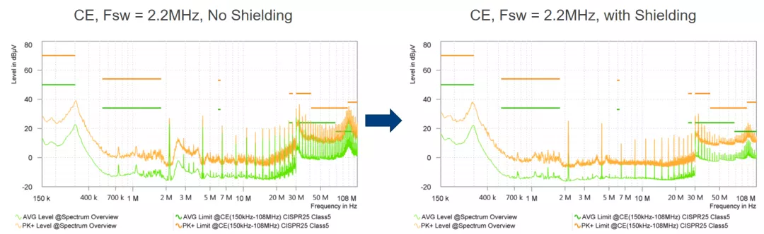
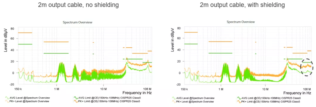
The EMI test results also verify that after adding the shield, the conducted noise significantly improves (see Figure 6). In the case a 2m output line, conducted noise can also meet the requirements of CISPR 25 Class 5, with a 6dB margin.
Practical Application with the MPQ7200
This article mostly analyzed long-line loads using a Class-D amplifier as an example, but these methods are applicable to other chips. For example, the MPQ7200 is a high-frequency, constant-current, buck-boost LED driver that uses several methods (i.e. frequency jittering and symmetrical VIN designs) to reduce EMI.
Figure 7 shows that when there is no output line, the conducted EMI noise is very low. When a 2m output line is added, however, conducted EMI has two resonant peaks at the corresponding position.

Figure 8 shows how adding a shield can reduce the MPQ7200’s conduction noise. This effect is pronounced at high frequencies, and indicates that the principles and noise reduction measures covered in this article are common across all converter topologies.
Conclusion
In summary, we developed a high-frequency CM model throughout Part I and Part II. This article compared three EMI reduction methods and examined the conducted EMI’s resonant peaks. As shown by these articles, excessive EMI under a long-line load can be effectively controlled for various automotive electronics applications by using strategic circuit modifications.
_______________________
Did you find this interesting? Get valuable resources straight to your inbox - sent out once per month!
Technical Forum
 Latest activity a day ago
 2 Comments
Latest activity 2 days ago
2 Comments
Latest activity 2 weeks ago
3 Comments
2 Comments
Latest activity 2 days ago
2 Comments
Latest activity 2 weeks ago
3 Comments
Log in to your account
Create New Account