Building Power Systems with the MP188xx Isolated Gate Driver Series

Get valuable resources straight to your inbox - sent out once per month
We value your privacy
Introduction
Power is essential to 5G communication, data centers, photovoltaic inverters, on-board power supplies, charging piles, and LED control systems. Across these power systems, an isolated gate driver is required to drive the switch tube efficiently and reliably for power conversion.
Isolated Gate Driver
An isolated gate driver is characterized by a small charger and large gate transmission. These drivers are widely used in high-power, high-voltage applications, insulation safety, and fast control. Figure 1 shows common power system applications for isolated gate drivers.
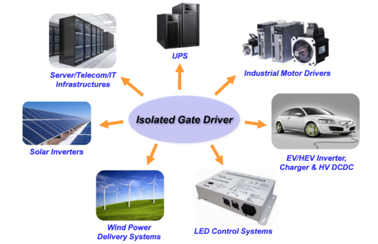
Figure 1: Common Power System Applications of Isolated Drivers
The isolator family typically includes photoelectric-isolated, transformer-isolated, and capacitive-isolated devices. In particular, photoelectric isolators have a long relative transmission delay, high distortion, and low channel-matching.
With the development of processes and the increasing emergence of new power devices (e.g. Si, IGBT, SiC, GaN, etc.), there are different requirements for switching frequencies and driving voltages. It is vital to select the optimal driver for each unique application.
The MP188xx Family
The MP188xx series are high-voltage isolated drivers, including the MP18831, MP18851, and MP18871. These devices offer two enable logics (enable and disable) and three package options: a narrow-body or wide-body SOIC-16 package (SOIC-16NB or SOIC-16WB, respectively), or an LGA-13 (5mmx5mm) package. Table 1 shows the main differences between the MP18831, MP18851, and MP18871.
Table 1: MP188x1 Comparisons
| PN | Description | Features |
| MP18831 | Isolated, dual-input, half-bridge gate driver | Overlap protection, adjustable dead time |
| MP18851 | Isolated, independent dual-channel gate driver | No overlap protection |
| MP18871 | Pulse-width modulation (PWM) input half-bridge gate driver | Overlap protection, adjustable dead time |
MP18831
The MP18831 integrates dual-input gate drivers in one package and features a configurable dead time. If the two inputs are high at the same time, then the output is low, which can protect the whole device. In addition, the MP18831 provides up to 4A of source and sink peak current capacity, and up to 5kVRMS of withstand voltage by utilizing our proprietary, capacitive-based isolation technology.
Figure 2 shows the MP18831’s typical application circuit.

Figure 2: MP18831 Typical Application Circuit
Figure 3 shows a power supply application example comprised of an active power factor correction (PFC), half-bridge LLC, and synchronous rectifier. In this scenario, the MP18831 functions as the high-side/low-side isolated gate driver.
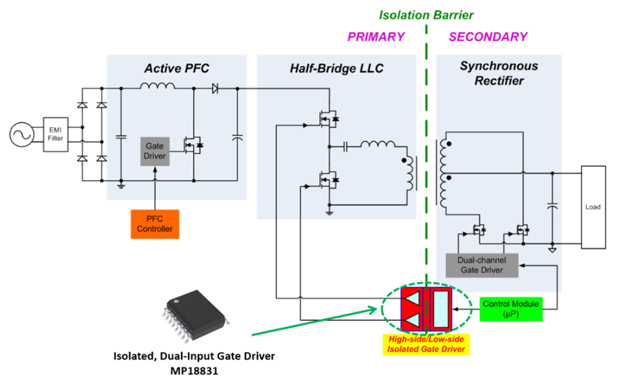
Figure 3: Power Supply Application Example with the MP18331
MP18851
The MP18851 is an independent dual-channel gate driver solution that can achieve simultaneously high outputs for either channel. The MP18851’s wide primary-side VDDI supply range allows the driver to be interfaced with 3.3V or 5V digital controllers. Its secondary-side driver accepts a supply up to 30V.
Figure 4 shows the MP18851’s typical application circuit.

Figure 4: MP18851 Typical Application Circuit
MP18871
The MP18871 in an isolated half-bridge gate driver. Its input terminal is a PWM signal, and it has up to a 0.5A or 4A source and sink peak current capacity. Figure 5 shows the MP18871’s typical application circuit.

Figure 5: MP18871 Typical Application Circuit
Advantages of the MP188xx Family
As a whole, the MP188xx series achieves excellent isolation and driving performance by adopting advanced capacitive isolation technology as well as fast and reliable on-off keying (OOK) transmission technology, with high reliability and wide compatibility.
When compared to traditional optocoupler gate drivers, the MP188xx series has several advantages such as low delay, low pulse-width distortion, strong common-mode transient immunity, long life, and a wide operating temperature range.
Table 2 shows the parameters of the MP188xx series.
Table 2: MP188xx Series Parameters
| Parameter | MP18831, MP18851, MP18871 |
| Input to output isolation |
|
| Functional isolation of two channel at the output |
|
| Common-mode transient interference (CMTI) | >100kV/µs, strong anti-noise ability |
| Input power supply (VDDI) range | 2.8V to 5.5V wide input, compatible with transistor-to-transistor logic (TTL) and complementary metal oxide semiconductor (CMOS) levels |
| Output power supply (VDDO) range | Maximum 30V supply voltage |
| Output under-voltage lockout (ULVO) section | 3V/5V/8V/10V/12V |
| Drive current capability | 4A source/sink maximum current output |
| Transmission delay | 50ns typical propagation delay |
| Operating temperature | -40°C to +125°C |
The other advantages of the MP188xx family include the following:
- Can drive power switching devices with a short propagation delay and low pulse-width distortion
- Provides overlap protection to prevent shoot-through
- The input side supports the CMOS and TTL logic inputs
- Features a 4A maximum drive current
- Available with a variety of output under-voltage lockout (UVLO) specification options
- CMTI exceeding 100kV/μs to ensure the reliable transmission of each PWM
Conclusion
In this article, we reviewed the features and advantages of the MP188xx family, a series of isolated gate drivers including the MP18831, MP18851, and MP18871. Isolated gate drivers are critical to driving switch tubes in power systems. To learn more about MPS isolation products, read our article on MPS’s isolated power solutions that promote carbon neutrality.
_______________________
Did you find this interesting? Get valuable resources straight to your inbox - sent out once per month!
Technical Forum
 Latest activity a day ago
 4 Comments
Latest activity a day ago
2 Comments
Latest activity 3 days ago
2 Comments
4 Comments
Latest activity a day ago
2 Comments
Latest activity 3 days ago
2 Comments
Log in to your account
Create New Account