Analysis and Modeling Method for Electromagnetic Interference (EMI) of Non-Isolated Converters (Part I)

Get valuable resources straight to your inbox - sent out once per month
We value your privacy
Introduction
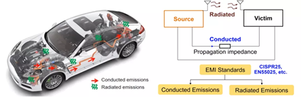
When designing an electronic system, ensuring the device meets electromagnetic compatibility (EMC) standards is crucial — not only because of the requirements placed by legislative bodies, but also because electromagnetic interference (EMI) can lead to instability and unwanted behavior. Since EMI testing usually takes place in the final design stages, being able to model and analyze EMI can effectively help designers optimize for EMI from the first design stages and throughout the design process, helping them avoid delays and unexpected costs.
EMI is propagated in an electronic circuit through two paths: conducted and radiated EMI. Conducted EMI is transmitted to the affected device through cables or other conductors with physical contact, while radiated EMI noise is transmitted through open space (no physical contact).
Because these propagation paths are different, this article series will address conducted EMI in part I, then it will address radiated EMI in part II.
Conducted EMI
There are two standard types of conducted EMI: differential mode (DM) and common mode (CM). DM noise flows between the two lines. CM noise is created when current flows to the ground in the form of a displacement current, which flows through the equipment’s stray capacitance to the ground, and then flows back to the power grid.
When measuring EMI noise, a noise separator can be used to determine whether the EMI noise is DM noise or CM noise (see Figure 1).

Figure 1: Common and Differential Mode Noise in Conducted EMI
When analyzing and modeling conducted EMI, it is vital to analyze DM noise and CM noise separately.
Figure 2 shows the DM and CM noise paths, where LF is the input filter’s inductance, and CF is the input filter’s capacitor. CP is the stray capacitance from the switch node, and CPO is the stray capacitance of the evaluation board’s ground to the test reference ground.
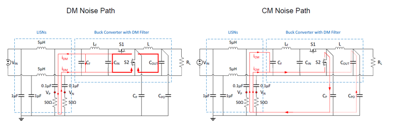
Figure 2: DM and CM Pathways of a Buck Circuit
Related Content
-
ARTICLE
EMI Generation, Propagation, and Suppression in Automotive Electronics (Part I)
This article provides modeling and suppression methods to reduce EMI in non-isolated converters, such as buck, boost, and buck-boost converters
-
WEBINAR

On-Demand EMC Workshop: EMI Troubleshooting and Debugging
Discover the fundamentals of practical EMI/EMC design and troubleshooting of electronic circuits, using state-of-the-art scopes to analyze your signals in both the time and frequency domains
-
VIDEO

Mythbusting EMC Techniques in Power Converters
Proven ways to improve EMC in your power converter design
-
ARTICLE
EMI Generation, Propagation, and Suppression in Automotive Electronics (Part II)
Part II covers radiated EMI modeling strategies based on Thevenin’s Theorem, as well as ground impedance reduction techniques
Differential Mode (DM) Noise
The substitution theorem can be used to calculate DM noise. This theorem states that the voltage or current across any branch can be replaced with various elements to make the same voltage and current. Figure 3 shows the buck converter circuit after replacing all switches (S1 and S2 in Figure 2) within the circuit for current or voltage sources (IS1 and VS2 in Figure 3). In this scenario, after branch equivalence, the circuit’s current and voltage are unchanged.
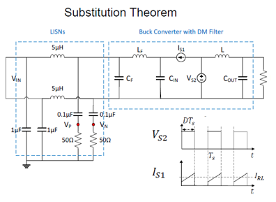
Figure 3: Modeling Analysis for DM Noise with the Substitution Theorem
The superposition theorem is used to analyze the influence of each power source on EMI (see Figure 4). This creates two circuits: one with the current source (IS1), and a second with the voltage source (VS2). Only the current passing through the LISN generates EMI, so any sources that do not generate EMI noise can be ignored. This means that only the circuit with the current source needs to be analyzed.
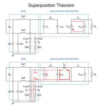
Figure 4: Modeling Analysis with Superposition Theorem
Figure 5 shows the DM noise model. This model shows that the source of DM noise is the high-side switch current (IS1). By analyzing the circuit in Figure 5, the DM noise current can be reduced by selecting an appropriate input capacitor and input filtering inductor (CF and LF, respectively).
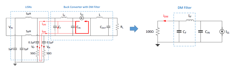
Figure 5: Buck Converter’s DM Noise Model
Common Mode (CM) Noise
Figure 6 shows how CM noise can be similarly analyzed using the substitution theorem and the superposition theorem. In this scenario, the source of CM noise is the low-side switch acting as a voltage source (VS2) (see Figure 6). Since CM noise is coupled through the PCB ground plane, CP and CPO must also be added. CP is the parasitic capacitance created by the switch node plane to the ground plane, which couples the switching noise, and CPO is the parasitic capacitance created by the output voltage plane to the ground plane, where the output voltage ripple can be coupled.
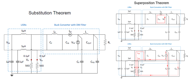
Figure 6: Modeling Analysis for CM Noise with the Substitution and Superposition Theorem
Figure 7 shows the CM noise model in a buck circuit. For CM noise, because the impedances of the input and output capacitors (CIN and COUT, respectively) are much smaller than CP and CPO, they can be considered a short circuit during analysis. CM noise can be reduced by selecting a lower-value CP, which stresses the importance of reducing the size of the switch node to make the CP capacitor as small as possible.
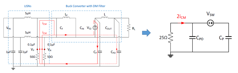
Figure 7: Buck Converter’s CM Noise Model
This analysis method can also be applied to other non-isolated converters, such as boost and buck-boost converters.
Passive Components
Although the above sections create a basic EMI model, designers should consider the influence of each component’s parasitic parameters to accurately predict high-frequency (e.g. exceeding 30MHz) EMI.
Figure 8 shows EMI-generating passive components that can commonly be found on switching power supply PCBs.
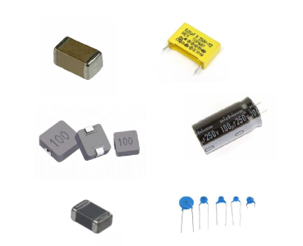
Figure 8: Common EMI Passive Components
Figure 9 shows the high-impedance model for capacitors. The current flowing though the capacitor creates a magnetic field around it, and the conductive material in the connectors act like a small parasitic resistor.
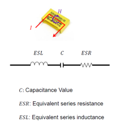
Figure 9: High-Frequency Equivalent Model of a Capacitor
Figure 10 shows the high-frequency impedance model for inductors, where the electric field generated between the inductor windings forms an equivalent capacitor, and the power losses caused by heating in the conductors can be treated as parasitic resistors in series and parallel.
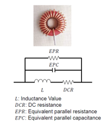
Figure 10: High-Frequency Equivalent Model of an Inductor
Typically, the supplier should provide any parasitic parameters that can be used to determine EMI noise, but if this information is not included, it can be measured with an impedance analyzer or a network analyzer.
When looking at the impedance profile of passive components, the evolution of the impedance has a triangular shape (see Figure 11). At very high frequencies, the parasitic inductor in capacitors causes the impedance to rise, so the capacitor exhibits inductive behavior. The opposite occurs for the inductor, with the parasitic capacitance and resistance becoming the main components of the impedance. In a switching converter, there are high-frequency components caused by the sharp changes in current and voltage in the circuit. For certain high-frequencies, designers must consider that the components they are using may respond differently from what they expect.
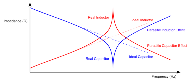
Figure 11: Frequency Impedance Profile of Inductors and Capacitors
Furthermore, when analyzing high-frequency EMI, the inductance generated by PCB traces cannot be ignored, and it must also be considered during EMI modeling. An impedance analyzer or a network analyzer can measure EMI components and extract stray parameters on the PCB. However, as a general design rule, it is recommended to make traces as short as possible, especially those that are noisy or susceptible to noise.
After analyzing EMI components and PCB stray parameters, the model from Figure 2 can be simulated (see Figure 12). The voltage and current on the switch can be obtained via real measurements, and it can also be simulated by using the model of the switch or IC in the simulation.
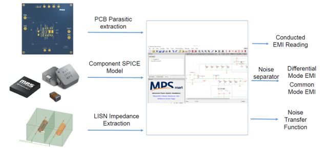
Figure 12: EMI Prediction using Simulation Software
Figure 13 shows that when accurately extracting EMI components and PCB impedance, an EMI simulation can accurately predict the converter’s conducted EMI result.
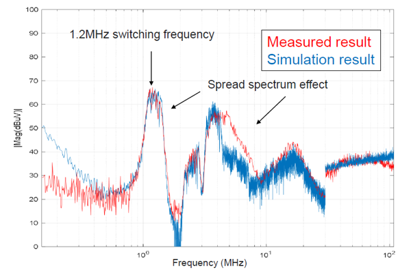
Figure 13: Comparison of EMI Simulation Results and Actual Measurement
Conclusion
This article described how to analyze EMI noise and create a modeling method for conducted EMI (DM noise and CM noise), as well as how passive components can also increase EMI, while using a buck converter and buck-boost converter as examples. Part II will discuss radiated EMI. MPS offers an extensive number of non-isolated switching converters and controllers as well as isolated converters to meet your application needs.
MPS also offers automotive-grade buck-boost converters and buck converters to meet stringent EMI requirements, in addition to EMC testing laboratories.
_______________________
Did you find this interesting? Get valuable resources straight to your inbox - sent out once per month!
Technical Forum
 Latest activity 21 hours ago
 4 Comments
Latest activity 21 hours ago
2 Comments
Latest activity 3 days ago
2 Comments
4 Comments
Latest activity 21 hours ago
2 Comments
Latest activity 3 days ago
2 Comments
Log in to your account
Create New Account