A Thermally Optimized, Two-Layer Automotive PCB Design to Meet CISPR25 Class 5

Get valuable resources straight to your inbox - sent out once per month
We value your privacy
Introduction
Automotive electronics suppliers are faced with escalating cost pressures in the race to produce autonomous, connected, and electrified solutions. One effective way to reduce design costs is by using 2-layer automotive PCBs. However, 2-layer PCBs require special care, as they can have poor thermal characteristics, which leads to compromised performance.
In this article, an automotive expert will use MPS’s MPQ4323-AEC1 to provide practical advice on how the schematic and layout designs for 2-layer PCBs can be fine-tuned to achieve the best possible thermal characteristics, and stay well within the standards for CISPR25 Class 5.
Using a 2-Layer Layout
The required number of layers depends on the PCB space and the number of components, as well as the planned production costs. A hardware designer often only has two available layers. In a 2-layer automotive PCB design, DC switching power supplies require careful component placement to meet EMC and thermal requirements.
Related Content
-
VIDEO

MPSafe™ Automotive Functional Safety Development
Meet our rigorous ISO26262-compliant functional safety product development process
-
APPLICATION BLOCK

Infotainment Systems
Our highly efficient power solutions provide everything you need to power the next generation of infotainment system designs
-
VIDEO
Make a Great Automotive PCB for EMC & Thermal
Learn how to design a 2-layer PCB that will pass automotive EMC and can effectively dissipate heat
-
ARTICLE
Using Thermal Derating to Extend Automotive LED Life Expectancy
Discover our LED driver solutions, such as the MPQ2489-AEC1
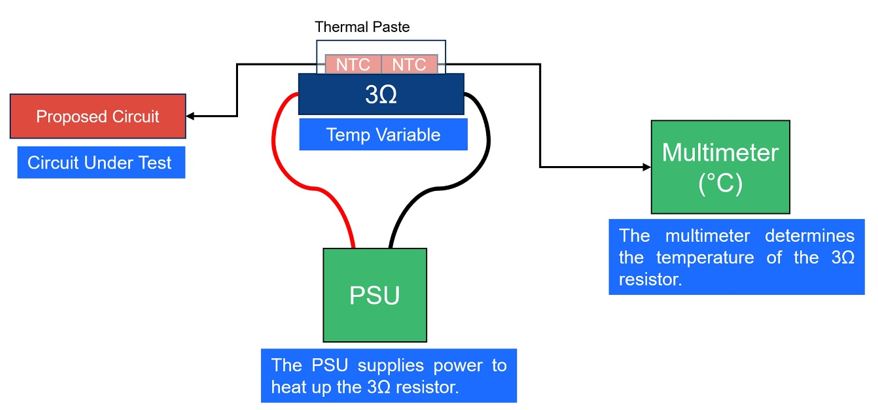
The Method
For this article, we tested nine 2-layer layouts. Each layout had unique component positions and slight modifications compared to the other PCBs, as well as different placements for the polygons and vias (see Figure 1). The purpose of using nine layouts was to find a successful solution with improved EMC and thermals. This article will focus on the differences between the thermal and EMC performances between these layouts.
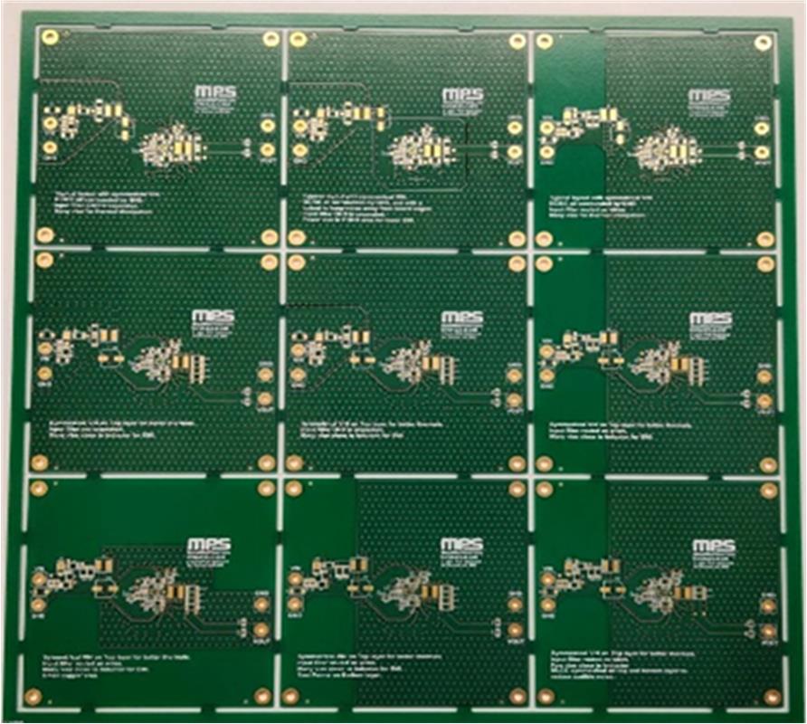
Figure 1: PCB Panel with Nine Different Layouts
Recommendations for a 2-Layer Layout
By following certain design rules, it is possible to achieve a solution that has been optimized for thermals and EMC. Figure 2 shows an example of a circuit using MPS’s MPQ4323-AEC1, a DC power switching supply that meets automotive EMC CISPR25 Class 5 requirements while using a thermally optimized 2-layer layout.
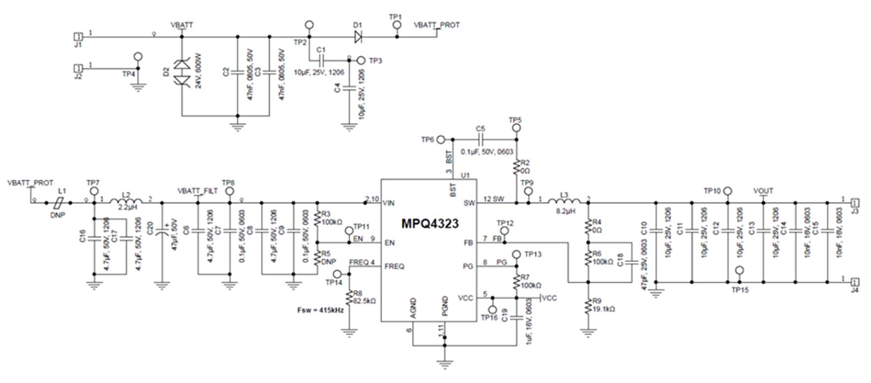
Figure 2: Thermally Optimized MPQ4323 Schematic that Meets Automotive EMC
Figure 3 shows the PCB component placement using the schematic from Figure 2.
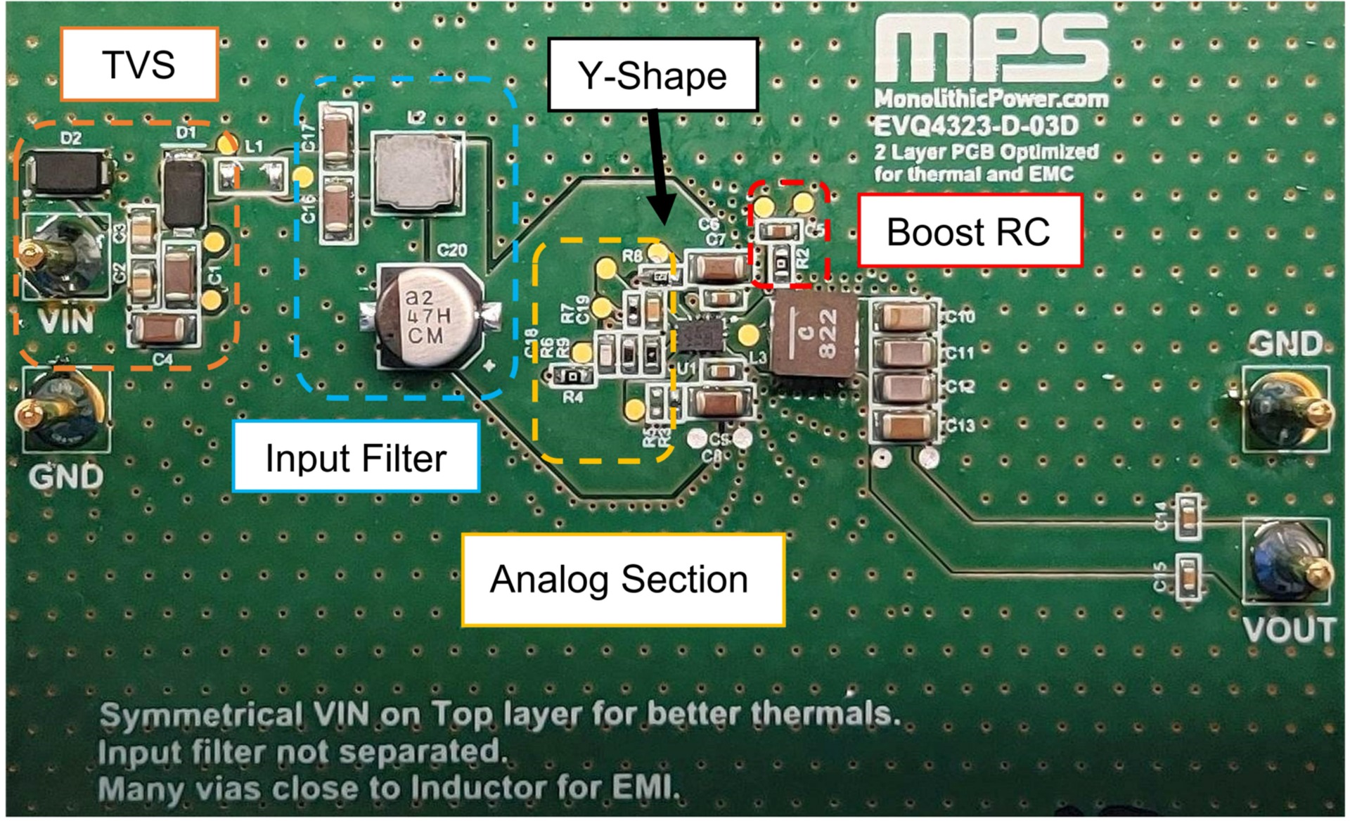
Figure 3: MPQ4323 2-Layer PCB Component Placement
The recommended layout has a solid top, bottom GND plane, and a large VIN polygon. It also utilizes PGND vias to connect the top and bottom layer. Figure 4 shows the solution’s thermal image. The Y-shaped VIN heatsink polygon extracts heat on the top layer. PGND vias are connected to the top and bottom layer to act as a second effective heatsink.
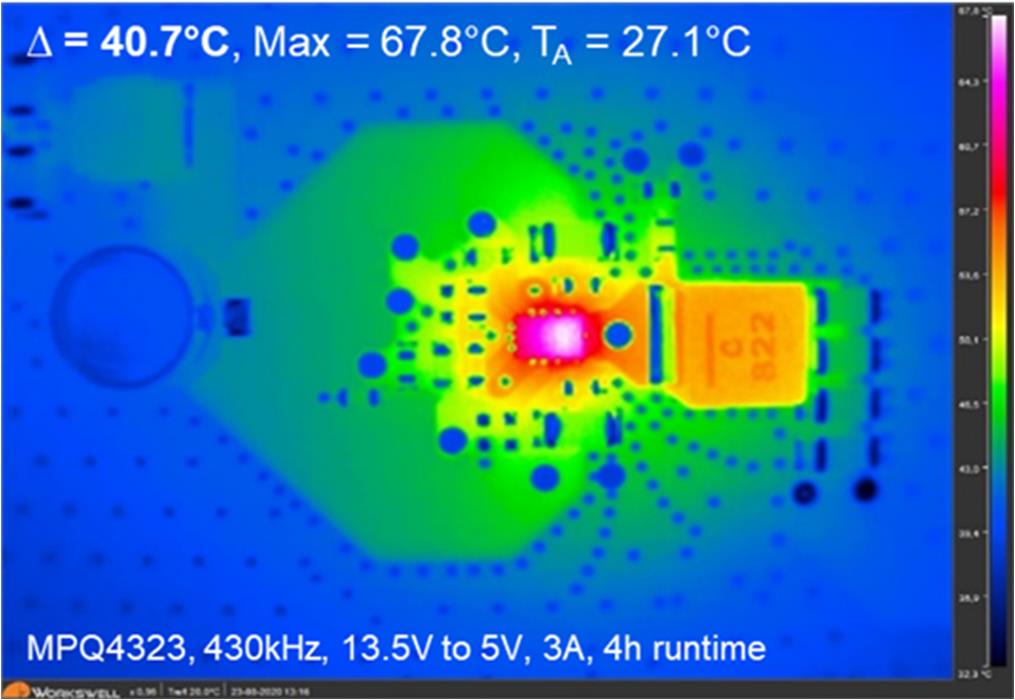
Figure 4: MPQ4323 2-Layer PCB Thermal Image
The inductor (L3) acts as effective heatsink (see Figure 4). In this example, the switchting node on pin 12 must have a small surface area so that it does not act as an emmitting antenna due to its fast-changing voltage (high du/dt). Place the inductor as close as possible to pin 12, as the short distance allows for optimal heat flow into the inductor. For excellent EMC, place the marked side of the inductor winding so that it aligns with pin 12. This allows the outer copper windings of the inductance to shield the inductor coil’s noisy inner area, which has a high du/dt. Figure 5 shows the heat distribution in the package.

Figure 5: MPQ4323 Heat Distribution in the Package
The most effective pins to transfer heat into the PCB are VIN, PGND, and SW. The internal lead frame connects these pins directly to the high-side and low-side MOSFETS (HS-FETs and LS-FETS, respectively). The lead frame is internally soldered under the die for effective heat flow.
The die is hotter closer to the MOSFET, since that is where the heat is internally generated. This effect can be seen on the white area on the package (maximum 67.8°C) when compared to the magenta area (about 62°C). The thermal conductivity of copper is 388W/mK, while that of silicon is 180W/mK. This means that heat distributes more evenly in copper. Note that the measured temperatures are on the package’s surface — the internal die temperature is hotter by a few degrees.
The analog pins (BOOT, VCC, AGND, FB, PG, and EN) do not have such efficient thermal conductivity when compared to the MOSFETs, whose inner length on the lead frame is shorter. Therefore, when designing the layout, the power pins (VIN, PGND, and SW) should have large copper surfaces to cool the device. The top layer near the power pins is the most effective heatsink.
A via that is placed between the top GND layer and the bottom GND layer has a more effective heat flow when it is closer to a power pin. It is recommended to place vias in the hotter locations. However, ensure that there are not too many vias placed next to each other. Too many holes can hinder the heat flow on the top layer due to the lack of copper.
It is important that the top layer has a direct copper connection for heat flow. The bottom layer deteriorates due to the thermal series connection with the vias. To improve thermal convection, it is recommended to place a DC power switching supply on the top layer.
Figure 6 shows a traditional layout with a cut in GND around the DC/DC converter. Meanwhile, VIN is connected on the bottom layer with a Y shape.
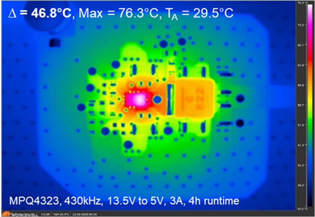
Figure 6: MPQ4323 in a Traditional Layout with Less Heat Flow into the PCB
Compare the temperature difference (ΔT) between the maximum TJUNCTION (white area) and TAMBIENT between both layouts. In Figure 4 (which is the thermally optimized recommended layout), ΔT 40.7°C. In the traditional solution, ΔT is 46.8°C.
The recommended layout runs 6°C colder than the traditional layout, all without using extra parts or a larger board space. This improvement is possible through the clever use of all five power pins, an enlarged VIN area, and sufficient PGND vias between the top GND and bot GND layer.
Comparing the MPQ4323-AEC1 to Similar Solutions
Figure 7 compares a solution (Solution 2) to the MPQ4323-AEC1. Note that both devices use the same IC package size, and both ICs operate on the same layout with the same external components.
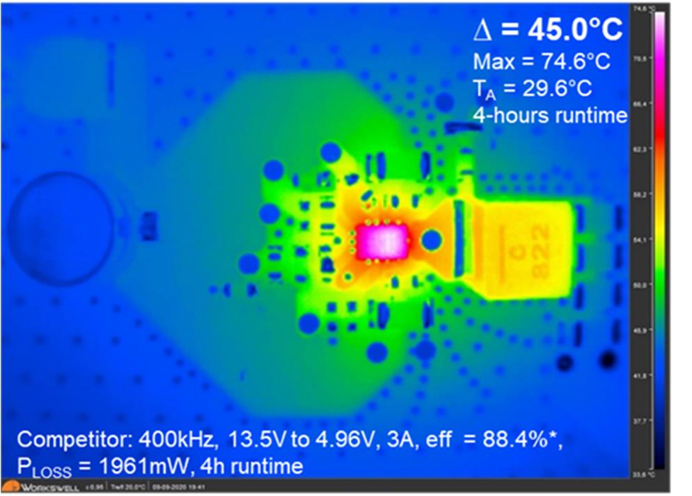
Figure 7: Solution 2 PCB Thermal Results
Table 1 lists the characteristics for both solutions.
Table 1: MPQ4323 vs. Similar Solution
| MPQ4323-AEC1 (Figure 4) | Solution 2 (Figure 7) | |
| ∆T | 40.7K | 45K |
| Switching Frequency (fSW) | 430kHz | 400kHz |
| Input Voltage (VIN) | 13.5V | 13.5V |
| Output Voltage (VOUT) | 4.93V | 4.96V |
| Output Current (IOUT) | 3A | 3A |
| Efficiency | 89.9% (1) | 88.4% (1) |
| Power Loss (PLOSS) | 1841mW during 4hr runtime | 1961mW during 4hr runtime |
Note:
1) The efficiency measurement includes the input filter, protection diode, and power inductor losses.
The lower temperature on the MPQ4323-AEC1 is the result of MPS’s advanced package technology, which allows for more heat to flow into the PCB.
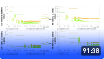
EMC Results
Figure 8 shows the EMC measurement CISPR25 Class 5 results for the MPQ4323-AEC1’s conducted emissions and radiated emissions between 150kHz and 30MHz.

Figure 8: Conducted Emissions (150kHz to 108MHz) and Radiated Emissions (150kHz to 30MHz) (Pass)
Figure 9 shows the EMC measurement CISPR25 Class 5 results for the conducted emissions and radiated emissions between 30MHz and 200MHz.
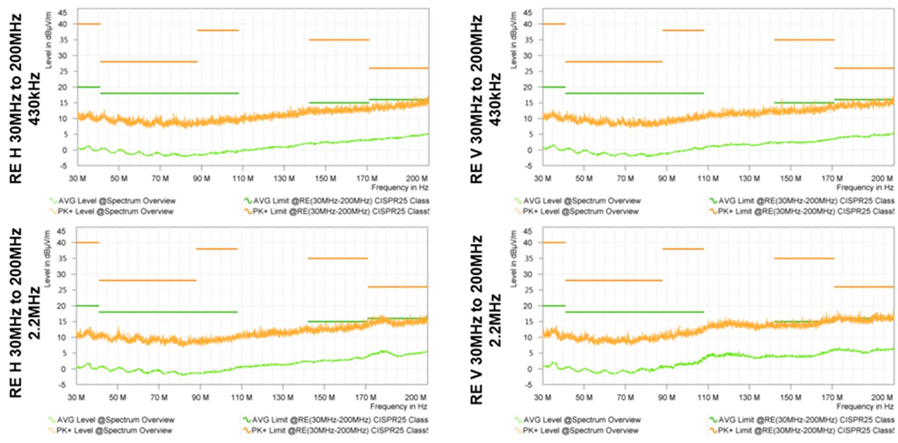
Figure 9: Horizontal Radiated Emissions (30MHz to 200MHz) and Vertical Radiated Emissions (30MHz to 200MHz) (Pass)
Figure 10 shows the EMC measurement CISPR25 Class 5 results for the conducted emissions and radiated emissions between 200MHz and 1GHz.
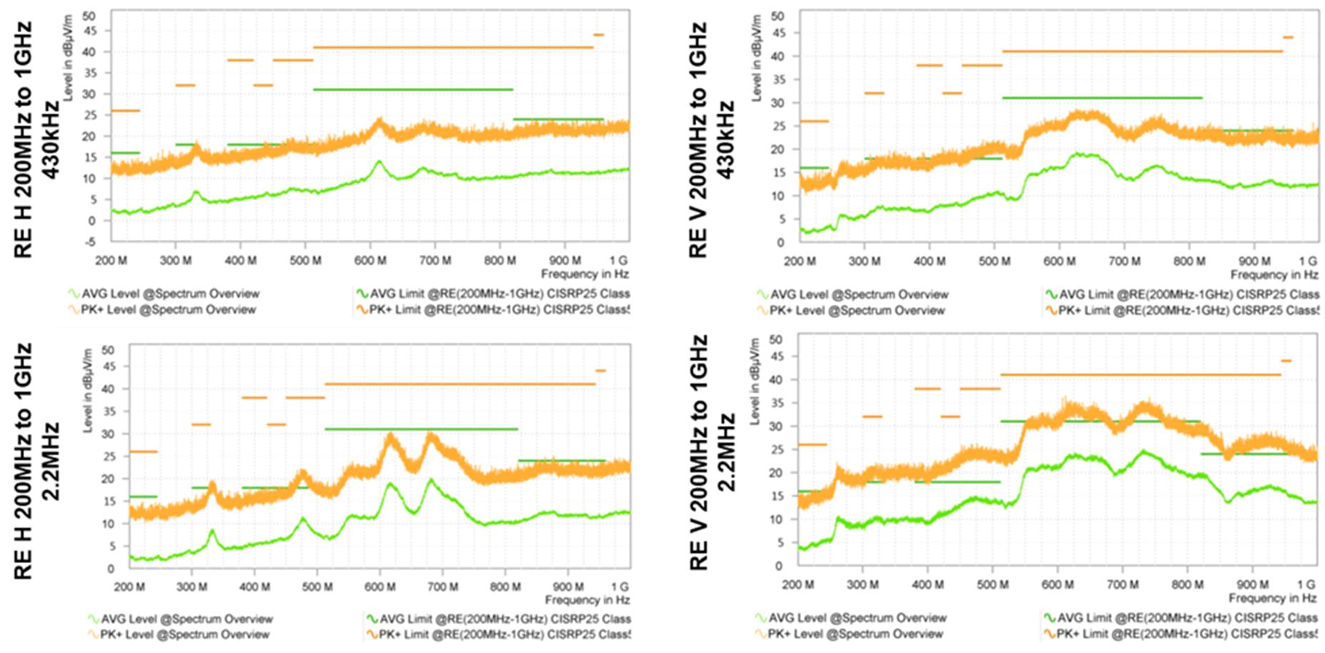
Figure 10: Horizontal Radiated Emissions (200MHz to 1GHz) and Vertical Radiated Emissions (200MHz to 1GHz) (Pass)
All EMC measurements are below the required limits, even though it typically a demanding task to pass automotive EMC requirements using only a 2-layer PCB. A 4-layer PCB is the common, standard solution for an automotive DC switching power supply, but a 4-layer layout increases costs. The methods in this article show that a 2-layer PCB can pass automotive EMC requirements while keeping the thermal rise low.
Recommended PCB Layout
Figure 10 shows the recommended PCB layout. The top layer shows the VIN Y-shaped polygon, which has a low impedance and noise. On the top layer, there are no vias and conductors placed near the IC. Vias from the top to bottom layer are only placed close to the power pins if there is heat flow.
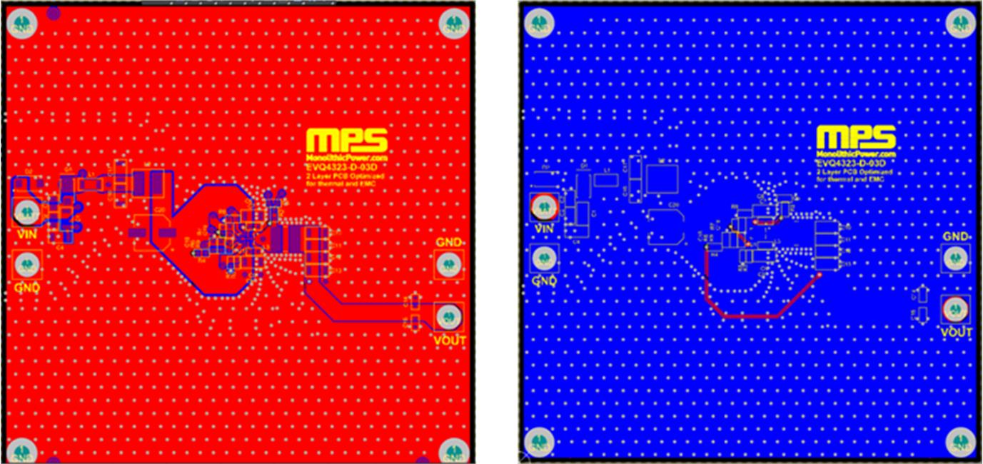
Figure 11: New Recommended Layout (Left: Top Layer; Right: Bottom Layer)
Excellent component placement results in only three traces between both layers (marked in red on the bottom layer). The longest trace is the VOUT sensing trace that goes to the FB feedback resistors. VOUT is quiet (good for EMC) and it is not sensitive to immunity. These traces are fully encapsulated in the bottom GND layer, which shields traces against EMC.
The VOUT trace between C13 and R4 should be routed away from the switching node to improve immunity against the switching node’s fast-changing e-field. The distance and the shielding within the GND layer reduce the coupling.
The most sensitive trace is between R6 and the feedback (FB, pin 7). This trace should be routed on the top layer, and it should be as short as possible (a few millimeters long). There should be a large, uninterrupted GND plane under the IC, which means that the three traces on the bottom layer should not cut the GND plane near the IC. Cutting a GND plane increases its impedance in relation to its frequency. An intact GND plane is the basis for good EMC and circuit performance.
Consider the following when designing a 2-layer automotive PCB:
- The top layer has better heat flow than the bottom layer.
- Vias placed close to a power pin have a better heat flow compared to vias that are further away.
Follow the guidelines below to optimize a 2-layer PCB:
- Maximize the copper area for the power pins, since they have the greatest effect on effective heat flow into the PCB.
- Give the power pins a higher priority than the analog pins for the heatsink.
- Place the marked side of the inductance as close as possible to the switching node, and minimize its copper area.
- Do not cut the cooling power polygons with conductor traces. This is particularly important in the immediate vicinity of the power pins, as this could greatly reduce the heat flowing from the pin into the PCB.
After considering each laid trace and how impacts the interference, emission, and immunity, choose the best possible position, trace width, and via connection accordingly.
Conclusion
It is possible to create a cost-effective, 2-layer PCB design that can perform well in harsh environments. A low-cost design can pass the EMI test with CISPR25 and OEM limits with sufficient margin, which we have demonstrated using the MPQ4323-AEC1. In this automotive PCB design, the IC can achieve close to full output operation under ambient temperatures that are approximately 100°C when operating at 400kHz, and approximately 80°C when operating at 2.2MHz when given a sufficient copper area for dissipation. MPS has designed a thermal enhanced lead frame for higher efficiency, resulting in a thermally superior solution that can work within compact and space-constrained systems.
_______________________
Did you find this interesting? Get valuable resources straight to your inbox - sent out once per month!
Technical Forum
 Latest activity a week ago
 3 Comments
Latest activity 2 weeks ago
2 Comments
Latest activity 4 weeks ago
4 Comments
3 Comments
Latest activity 2 weeks ago
2 Comments
Latest activity 4 weeks ago
4 Comments
Log in to your account
Create New Account