Integrated Solution for Multiple Li-Ion/Li-Polymer Batteries

Get valuable resources straight to your inbox - sent out once per month
We value your privacy
Electrical equipment such as industrial medical equipment, robot vacuums, drones, and high-power speakers need multi-cell battery chargers for power. The traditional solution for multi-cell battery chargers is composed of several discrete power MOSFETs and multiple auxiliary components.
Figure 1 shows that in a traditional solution, designers need at least two power MOSFETs for a power converter, and one power MOSFET to prevent battery power from flowing back to the input. Control loops that include sensing circuits, compensating circuits, PWM generators, and drivers are essential. Furthermore, the system needs circuits that offer protection, indications for the input source or any changes in operating conditions, and other functions.

Figure 1: Traditional Solution for Multi-Cell Battery Chargers
These discrete components result in a complicated design process, high failure rates, large board size, and high BOM costs. The traditional solution needs improvement.
To increase product quality, reduce failure rates, and save on design costs, an integrated solution is a necessary evolution. A semi-integrated or fully integrated solution can solve issues traditional solutions face for multi-cell battery chargers and accelerate time-to-market.
Figure 2 shows a semi-integrated solution. In this solution, all control loops (including protections and indications) are integrated into a dedicated IC. This eliminates the need to design compensation parameters, write complicated codes, or draw complex PCB layouts, which shortens the design process. However, discrete MOSFETSs still lead to a problem with board size.
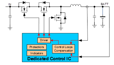
Figure 2: Semi-Integrated Solution
In a fully integrated solution, three power MOSFETs with low conduction resistance and all the control loops are integrated in one device (see Figure 3). This significantly shortens the design process, reduces BOM size, and optimizes efficiency.
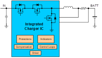
Figure 3: Fully Integrated Solution
Table 1 lists the BOMs integrated versus traditional solutions. Integrated solutions (especially ones that are fully integrated) greatly reduce board size.
| Component | Fully Integrated | Semi-Integrated | Traditional |
| Charger IC | 1 | 0 | 0 |
| Power MOSFET | 0 | 3 | 3 |
| Inductor | 1 | 1 | 1 |
| Sensing Resistor | 1 | 2 | 2 |
| Dedicated control IC | 0 | 1 | 0 |
| Driver | 0 | 0 | 3 |
| Amplifier and comparator | 0 | 0 | Several (5 to 10) |
| MCU | 0 | 0 | 1 |
| Total large component count | 3 | 7 | 15 to 20 |
Table 1: BOMs of Integrated Solutions vs. Traditional Solution
Innovation
Fully integrated multi-cell battery chargers have many advantages. For example, MPS’s MP2759 is a highly integrated switching charger designed for charging applications with 1-cell to 6-cell series Li-ion or Li-polymer battery packs. This IC integrates three power MOSFETs plus analog control circuits into a 3mmx3mm package, and can operate reliably and safely with very few external circuits.
Fully Integrated Charging System
Figure 4 shows a typical application circuit for a fully integrated solution. Its power stage needs one inductor and three capacitors, and with few external components, the complete charging function is realized.

Figure 4: Fully Integrated Solution Typical Application Circuit
A modern battery charger charges the battery pack in four phases: trickle charge, pre-charge, constant-current charge, and constant-voltage charge (see Figure 5). With all the control loops integrated in the device, charging is fast, simple, and reliable.
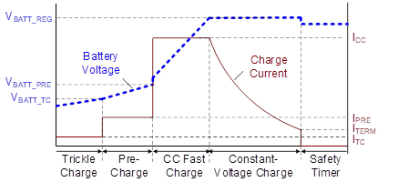
Figure 5: Typical Charge Profile
Thanks to the low conduction resistance of the integrated MOSFETs, fully integrated solutions such as the MP2759 boast high efficiency up to 97% (see Figure 6). These solutions can also offer outstanding thermal performance like the MP2759 with a case temperature rise of 42.3°C (see Figure 7).

Figure 6: Figure 6: Efficiency Curve of the MP2759
(Test Conditions: L = 10µH/35mΩ, RSNS = 20mΩ)

Figure 7: Thermal Performance Evaluation
(Test Conditions: VIN = 36V, VBATT = 24V, ICC = 2A, fSW = 700kHz, L = 10µH/35mΩ, RSNS = 20mΩ, burn in 20 minutes)
(Board Information: 63.5mmx63.5mm, 4-layer, 2oz./layer)
Function Extension with Simple External Circuit
Power Path Management
Ideally, integrated solutions should support power path management in order to prioritize power to the system rail. The MP2759 employs one common method for power path management. With an external P-channel MOSFET connected between the battery and the system, also known as a BATTFET, the system load is applied on the PMID pin, and the BATTFET’s gate is driven by the IN pin signal (see Figure 8).

Figure 8: Power Path Management
When there is no input source, the BATTFET turns on and current flows from the battery to the system. When an input source is present, the BATTFET turns off, and the system’s power is supplied by the input source through Q1. If the total input current through Q1 reaches the preset input current limit set by the ILIM pin, the charging current reduces to prioritize the system load.
As a demonstration, Figure 9 and Figure 10 show waveforms depicting the performance of the power path management in the MP2759.


Figure 9: Power Path Management Start-Up and Shutdown
(Test Conditions: VIN = 16V, VBATT = 8V, IIN_LMT = 2A, ICC = 3A, ILOAD = 1A)
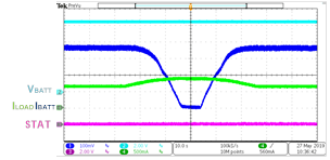
Figure 10: IIN_LMT Reaches the Preset Input Current Limit in Power Path Management
(Test Conditions: VIN = 36V, VBATT = 8.48V, IIN_LMT = 1A, ICC = 2A)
Fine-Tuning the Charging Current in Real Time with an MCU
Many battery-powered devices must be able to adjust the charging current in real time to fine-tune their performance. This is because battery cell and pack manufacturers specify different charge current limits, depending on the temperature and voltage of each cell. Most integrated multiple-cell battery chargers use a resistor connected to a current-setting pin (commonly called an ISET pin) to regulate the charging current, rather than use a more expensive I2C.
There are two common methods to regulate the charging current with one resistor:
- The current flowing through the resistor is read with a constant voltage.
- The voltage is read on the resistor while the current remains constant.
Let’s explore how to regulate the charging current in real time using an integrated charging solution based on method 1. Figure 11 shows the equivalent circuit of an ISET pin.

Figure 11: Equivalent Circuit of ISET Pin
The charger can regulate the charging current with a resistor (RISET) between the ISET pin and AGND. ICHG can be calculated with Equation (1):
$$I_{CHG} = \frac{R_{CONS}}{R_{ISET}}$$Where RCONS is the value of RISET when ICHG = 1A.
From the equivalent RISET circuit (see Figure 12), it is feasible to change the equivalent RISET by modifying the PWM’s duty cycle with an MCU. This allows the charging current to be changed in real time.

Figure 12: Equivalent RISET Circuit
Next, the equivalent RISET (REQ) can be calculated with Equation (2) and Equation (3):
$$R_{EQ} = \frac {V_{CONS} R_1 G_{123}}{V_{CONS} G_{123} - (\frac {DUTY × V_{M\_PWM}}{R_2} + \frac {V_{CONS}} {R_1})}$$ $$G_{123} ={1 \over R_1} + { 1 \over R2} + {1 \over R_3}$$Where VCONS is the constant voltage of ISET pin, DUTY is the PWM duty cycle, and VM_PWM is the PWM amplitude (usually about 3.3V). Note that in Equation (1), (2), and (3), REQ must be greater than 0; otherwise, ICHG is 0A.
To design a fully integrated system, standard parameters (R1, R2, R3, CISET) can be estimated with the following equations and steps:
First, the equivalent resistor corresponding to the maximum charging current (RMAX_ICHG) is calculated with Equation (4):
$$R_{MAX\_ICHG} = R1 + R2 / R3 $$Then choose an appropriate R1 using Equation (5):
$$R_{1} = 0.5R_{MAX\_ICHG}$$Next, R2 and R3 can be calculated with Equation (6):
$$ \biggl\{ \begin{array}{1} R_2//R_3 = R_{MAX\_ICHG} -R_1\\ \frac {MAX\_DUTY \space x \space V_{M\_PWM} - V_{CONS}}{R2} = \frac {V_{CONS}} {R_3} \end{array} $$Where MAX_DUTY is the maximum PWM duty when the charging current drops to 0A. It is recommended to be about 80% of the duty cycle.
Finally, choose an appropriate CISET to filter the PWM signal to the DC signal. CISET can be estimated with Equation (7):
$$ \frac {1}{2\pi (R_2//R_3)C_{ISET}}<< f_{PWM}$$Where fPWM is the PWM frequency.
An ideal solution for Li-ion and Li-polymer batteries should offer good linearity between the charging current and PWM duty cycle, and a wide duty effective range. For example, the MP2759 offers a range of 0% to 82% (see Figure 13).

Figure 13: Charging Current vs. PWM Duty Cycle
Additionally, the MP2759 does not experience overshoot or undershoot when the charging current changes (see Figure 14). The device demonstrates normal start-up and shutdown when the PWM duty cycle is 50% (see Figure 15).

a) PWM Duty Cycle Falls 65% to 10%

b) PWM Duty Cycle Rises 10% to 65%

a) VIN Start-Up
Figure 14: Charging Current Transition between 0.5A and 2.4A

b) Charge Enabled

c) Charge Disabled
Figure 15: Start-Up and Shutdown Waveforms with 50% PWM Duty Cycle
Functions – Protections and Indications
For charging systems and ICs, it is vital to protect the battery. To guarantee safe operation, recommended protections include battery and input over-voltage protection, battery temperature protection, thermal shutdown, a safety timer, and the ability to regulate the charge current depending on battery voltage. Fully integrated protection circuits reduce the number of ICs required for such protections.
The MP2759 has ACOK and STAT pins that indicate the input source status and the IC operation status. Designers can monitor the signals on these pins to determine whether the device is charging normally. Table 2 shows the ACOK and STAT statuses under different input sources and operating conditions.
| IN | Charging State | ACOK | STAT |
| Absend | NA | Hi-Z | Hi-Z |
| Present | In charging | Low | Low |
| Present | Charging complete, charging disabled | Low | Hi-Z |
| Present | NTC fault, safety timer expiration, battery OVP | Low | Blinking at 2Hz |
Conclusion
Compared to a traditional solution, a fully integrated solution offers very high efficiency, numerous safety features, lower BOM costs, and shorter design cycles. This article uses MPS’s MP2759 to demonstrate the advantages of an integrated solution, which includes three power MOSFETs with low conduction resistance, analog control loops, and auxiliary functions such as protections and indications. Integrated solutions such as this can help designers achieve power path management and charging current adjustment in real time with simple external circuits.
_________________________
Did you find this interesting? Get valuable resources straight to your inbox - sent out once per month!
Technical Forum
 Latest activity a day ago
 1 Comment
Latest activity 4 days ago
1 Comment
Latest activity a week ago
5 Comments
1 Comment
Latest activity 4 days ago
1 Comment
Latest activity a week ago
5 Comments
Log in to your account
Create New Account