EMI Generation, Propagation, and Suppression in Automotive Electronics (Part II)

Get valuable resources straight to your inbox - sent out once per month
We value your privacy
Introduction
This article is the second part of a two-part series delving into strategies for modeling and analyzing EMI problems. Part 1 explored approaches to reducing conducted EMI between differential mode (DM) noise and common mode (CM) noise. Part II will cover radiated EMI modeling strategies based on Thevenin’s Theorem, as well as ground impedance reduction techniques.
Radiated EMI
Traditionally, radiated EMI has been derived and analyzed using the electromagnetic field theory. However, for engineering applications, there are a limited number of complex formulas that can understand and solve EMI issues.
Another method to mitigate EMI problems is to establish a clear circuit model. Figure 1 shows how radiated EMI propagates through a dipole antenna that consists of input and output power cables. In this scenario, the converter’s CM noise source is the driving source for EMI.
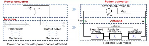
Figure 1: Mechanism and Model of Radiation EMI Generation
According to Thevenin’s Theorem, the converter can be modelled as a voltage source and its series impedance. Meanwhile, the antenna can be modelled with three impedances (RL, Rr, and XA) to represent its own power dissipation, the radiated energy, and the near-field energy stored by the antenna, respectively. We will further examine the converter and the antenna below.
Converter
Figure 2 shows that the weaker a converter’s source, the less energy it radiates. Ideally, there is no impedance between the input and output of the non-isolated converter, as the ground impedance is ignored. In this case, the equivalent source (VCM) is zero, and no EMI radiation is produced. In practice, however, the PCB trace between the ground produces inductance, and a voltage drop is generated between the input (P1) and the output (P3), which produces radiated EMI.

Figure 2: Ideal and Actual Buck-Boost Converter Circuit Model
With this knowledge, we can create a model for radiated EMI. Similar to the conducted EMI model, the voltage source and current source are used to substitute the active switches, based on the substitution theorem. Figure 3 shows that both the voltage source and the current source generate EMI noise, where a is the voltage source (VSW) and b is the current source (ID).
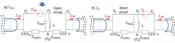
Figure 3: Buck-Boost Converter Radiates EMI Noise Source
Based on the model in Figure 3, the transfer function from each source to the equivalent CM source can be obtained. In this experiment, the voltage source and current source are measured by an oscilloscope; the magnitude of each impedance is measured by an impedance analyzer; and the equivalent source is predicted by calculations. Figure 4 shows that the forecasted values match the measured values of the equivalent CM source, thus verifying the model’s rationality.
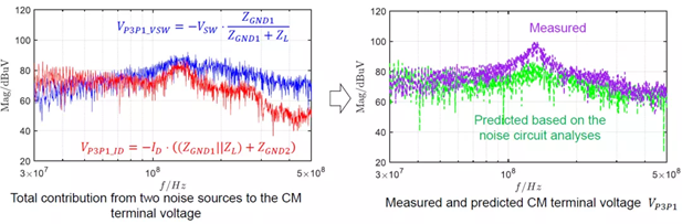
Figure 4: Comparison between the Predicted and Measured Equivalent CM Source
Antenna
A fixed antenna transfer gain is measured based on the antenna’s location and length, which are fixed in EMI tests. Using the equivalent CM source and impedance obtained in the previous section, the next step is to predict actual EMI noise. Figure 5 shows the process for predicting the EMI noise of a buck-boost converter. Figure 5a shows the radiated EMI prediction procedure, and Figure5b shows how the predicted results compare with the measured results. The comparison confirms that the predicted and measured radiated EMI noises are almost identical.
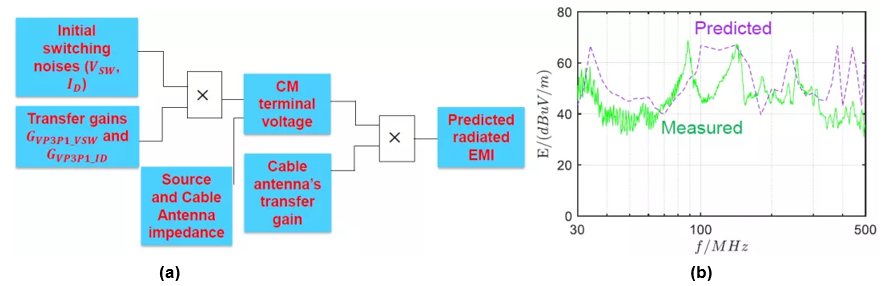
Figure 5: Procedure for Radiated EMI Prediction and Comparison of the Predicted and Actual Radiated EMI Noise
An effective method to suppress radiated EMI is to reduce the ground impedance. There are two reduction techniques that are general methods for non-isolated converters. The first technique is minimizing the distance between the input and output, which consequently reduces the ground trace impedance. The second technique is to add a small bypass capacitor between the input and output nodes to reduce the impedance between the input and output (see Figure 6).
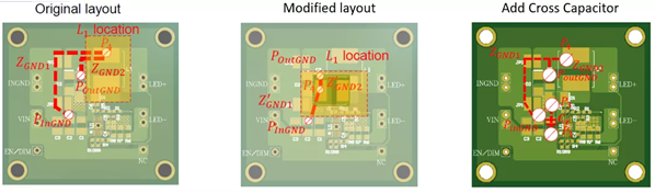
Figure 6: Reducing EMI by Modifying the PCB Layout
Figure 7 confirms the validity of these techniques. Figure 7a shows the original EMI results compared to the EMI results after modifying the PCB layout between the input and output nodes, while Figure 7b shows the EMI results after adding a crossing capacitor. Both techniques are able to reduce EMI.
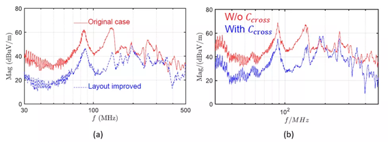
Figure 7: Reducing EMI with an Improved PCB Layout and a Cross Capacitor
Conclusion
This article reviewed methods for controlling radiation EMI noise by establishing the physical significance of the circuit model using the converter and antenna. When it comes to EMI issues, modeling and analysis approaches are vital because they enable automotive electronics engineers to meet EMI requirements and enhance safety standards for automotive electronics.
Did you find this interesting? Get valuable resources straight to your inbox - sent out once per month!
Technical Forum
 Latest activity a week ago
 2 Comments
Latest activity 2 weeks ago
4 Comments
Latest activity 4 weeks ago
2 Comments
2 Comments
Latest activity 2 weeks ago
4 Comments
Latest activity 4 weeks ago
2 Comments
Log in to your account
Create New Account