Domain Control Module - Automotive Power Stage for ADAS Applications

Get valuable resources straight to your inbox - sent out once per month
We value your privacy
1 Overview
1.1 Description
Advanced driver assistance systems (ADAS) have experienced an astonishing evolution over the last few decades, and today’s cars incorporate a large number of sensors and cameras that monitor every part of the vehicle, as well as its surroundings. As a consequence, the power requirements of these systems has increased, bringing new challenges to the power supply design. This reference design serves as a guideline to help users design a power supply for ADAS, using a domain control module as an example.
A key part of an ADAS power design is how it handles the transient voltage perturbations in the car’s battery. The initial voltage spike is especially critical, as some ADAS subsystems must remain operational even under cold start (also called cold crank) conditions. Under these conditions, the input voltage supply can fall to as low as 2.5V. The load dump can also be dangerous, as it can increase the power dissipation in lossy converters like LDOs.
To ensure that the system operates normally regardless of the input voltage range (while protecting the circuit’s components), it is vital to use a buck-boost converter rated for 42V. An example that meets this specification is the MPQ8875A, which will be discussed in this reference design.
1.2 Features
- Wide 2.2V to 36V Operating Input Range
- 15W to 20W Available Total Output Power During Start Impulse
- 4 LDO Channels for Power Over Coaxial with up to 300mA Each
- 4 LDO Channels with Monitoring, Diagnosis, and Protection Features
- Up to 1A of Continuous Output Current at 5V, or 3.3V for Auxiliary Devices (CAN, MCU)
- Buck-Boost and PoC LDOs are Configurable via the I2C Interface and OTP Memory
- Reverse Polarity Protection According to ISO 16750
- CISPR25 Class 5 Compliant
- All Parts Available in AEC-Q100 Grade 1
1.3 Applications
- Advanced Driver Assistance Systems (ADAS)
- Sensor Fusion Systems
- Camera Monitoring Systems
- Information Systems
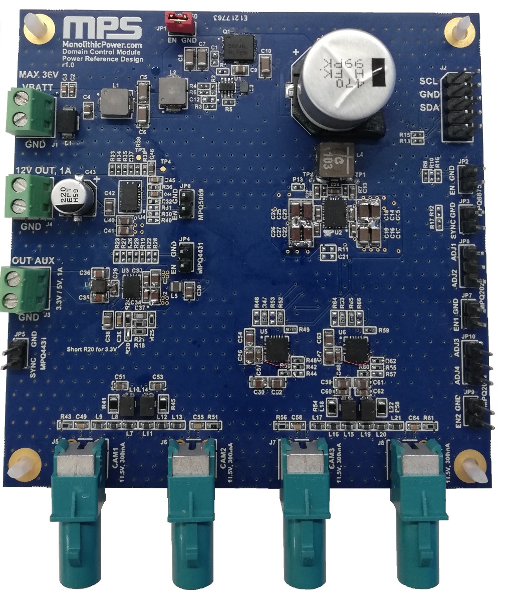
Figure 1: Domain Control Module Reference Design Board
Reference Design
2.1 Block Diagram
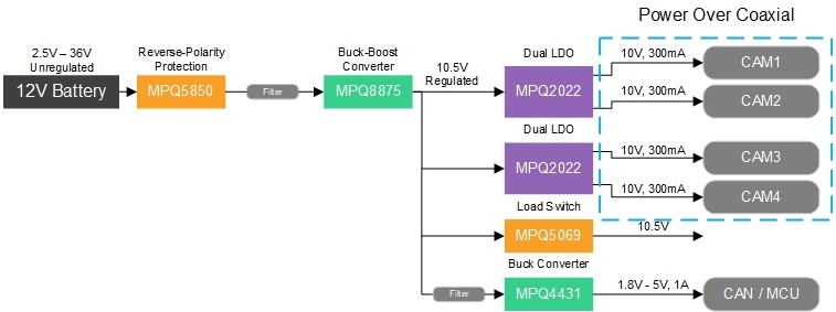
Figure 2: Block Diagram
Figure 2 shows a block diagram for this system. First, a battery supplies power to the MPQ5850, a smart diode controller that can protect the entire system from reverse input voltages, and rectify any AC voltages superposed on the supply line. Then the MPQ5850 powers the MPQ8875A, a 4-switch, synchronous buck-boost converter that can accommodate the input line transient voltages. The MPQ8875A supplies a stable voltage level to four power devices: two dual-channel LDOs, a load switch, and a buck converter.
The two MPQ2022 devices each provide two LDO channels. The MPQ2022s can supply a current up to 300mA to cameras and sensors through a coaxial cable with an excellent power supply rejection ratio (PSRR). These devices also have an analog-to-digital converter (ADC) and digital diagnostic features. The system also contains the MPQ5069, a load switch that enables an additional regulated output voltage that can be connected to additional ECUs. Lastly, the MPQ4431 is a compact buck converter that can supply 1A to auxiliary devices, such as a microcontroller (MCU) or a CAN driver.
2.2 Related Solutions
This reference design is based on the following MPS solutions:
| MPS Integrated Circuit | Description |
| MPQ5850 (1) | Smart diode controller with ultra-low dropout voltage for reverse input protection |
| MPQ8875A | Synchronous buck-boost DC/DC converter with I2C interface |
| MPQ2022 (1) | Dual-channel (LDO) with I2C interface |
| MPQ5069 | Hot-swap protection device designed to protect output circuitry from input transients |
| MPQ4431 | Synchronous step-down converter with internal high-side and low-side MOSFETs |
Table 1: System Specifications
(1) This part will be available soon. Contact us for details.
2.3 System Specifications
| Parameter | Specification |
| Input voltage range | 2.5V to 36V |
| Buck-boost output voltage | 10.5V |
| PoC output voltage | 10V |
| PoC maximum load current | 300mA per channel |
| MPQ4433 maximum load current | 1A |
| Switching frequency | 400kHz (under nominal conditions) |
| MPQ4433 output voltage range | 3.3V to 5V |
| MPQ5069 output voltage | 10.5V |
| MPQ8875A efficiency (VIN = 12V) | 98.96% (IOUT = 1A, VOUT = 10.5V) |
| Board form factor | 90mmx90mmx1.6mm |
Table 2: System Specifications
| Output Voltage | Maximum Output Current |
| 3.3V | 4.3A |
| 5V | 4.1A |
| 8V | 2.8A |
| 10V | 2.1A |
| 12V | 1.8A |
Table 4: Maximum Output Current vs. Minimum Input Voltage (MPQ8875A)
(VOUT = 10.5V, Room Temperature, Cold-Crank Profile)
| Minimum Input Voltage | Maximum Output Current |
| 2.5V | 1.42A |
| 3V | 1.9A |
| 3.5V | 2.2A |
| 4V | 2.6A |
| 4.5V | 3.1A |
| 5V | 3.5A |
| 5.5V | 3.9A |
| 6V | 4.2A |
| 6.5V | 4.5A |
| 7V | 4.8A |
Table 3: Maximum Output Current vs. Output Voltage (MPQ8875A)
(VCOND_MIN = 3.2V, Room Temperature, Cold-Crank Profile)
Test Results
3.1 Efficiency and Regulation
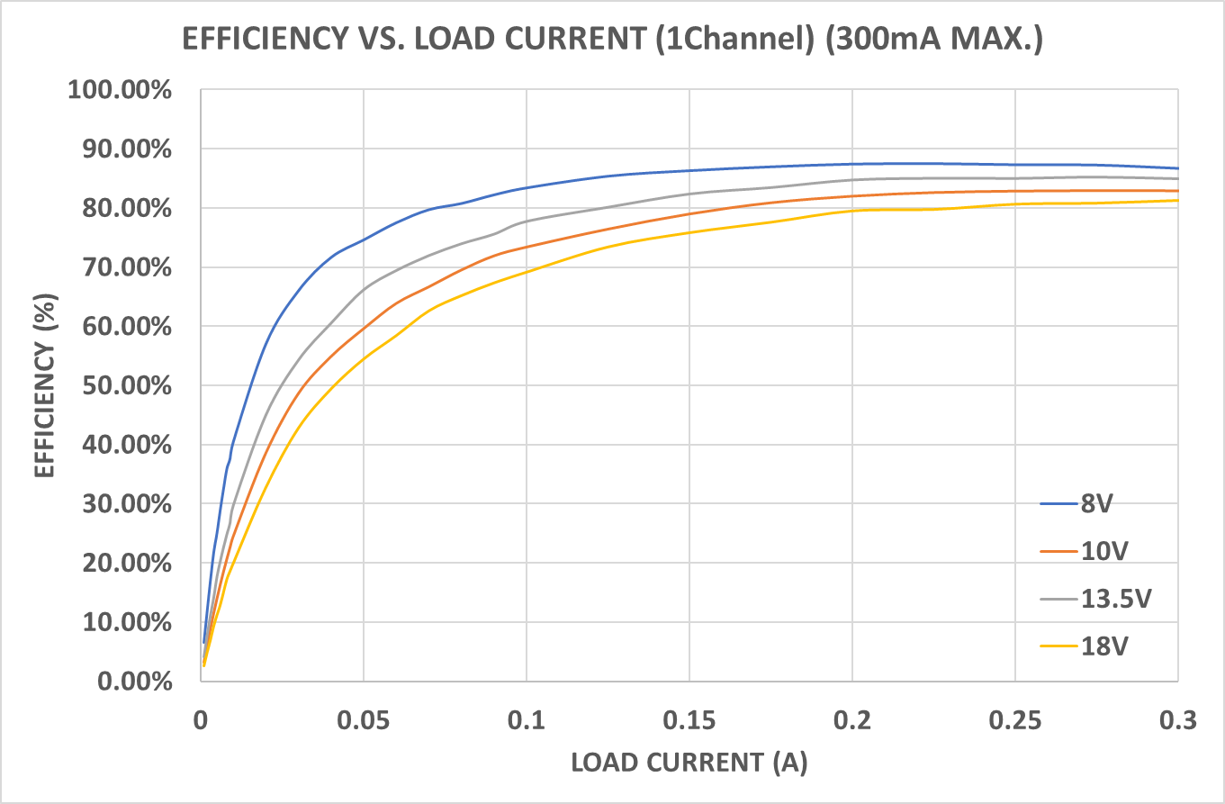
Figure 3: Efficiency vs. Load Current - System with one LDO channel connected
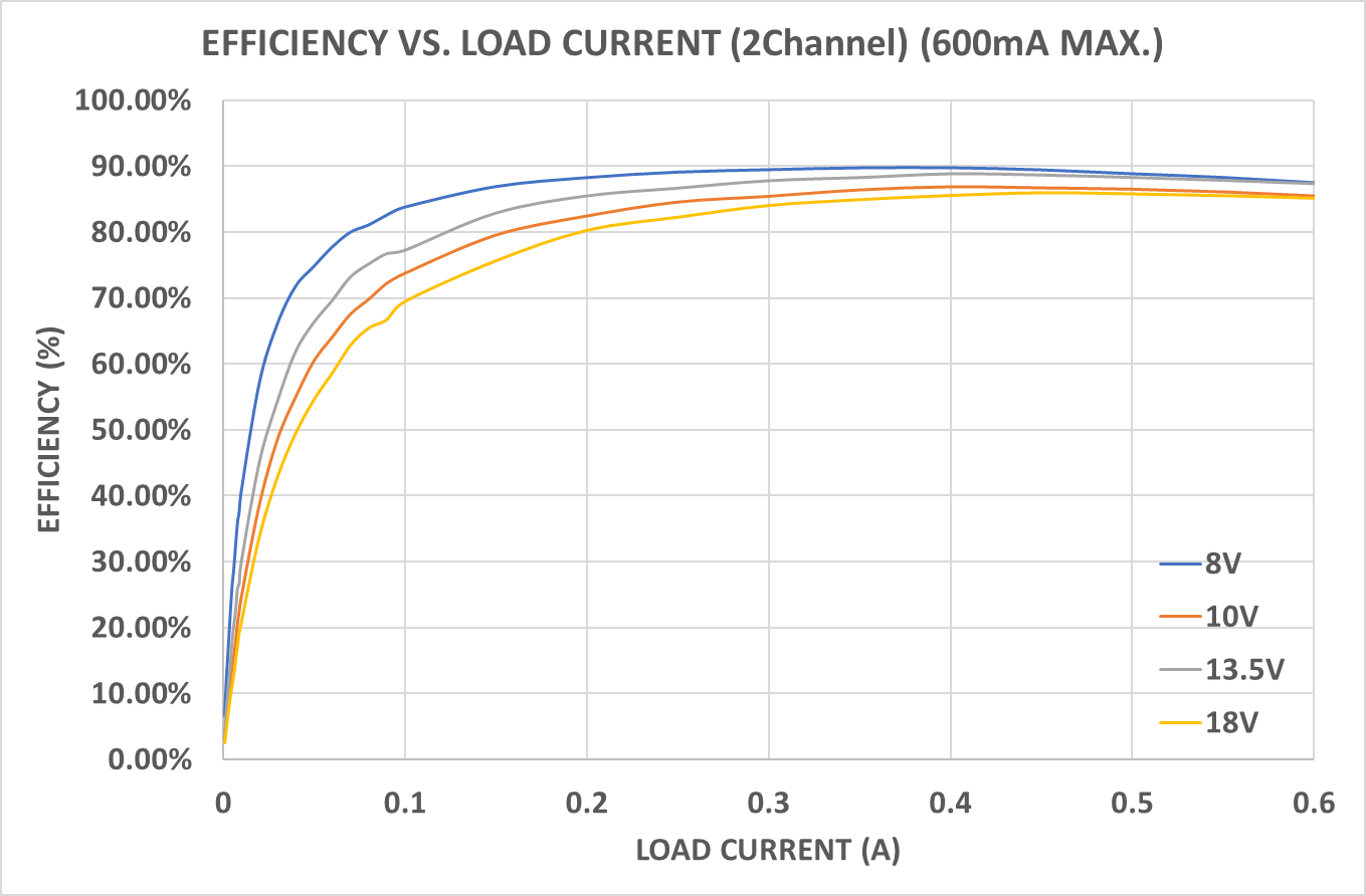
Figure 4: Efficiency vs. Load Current - System with two LDO channels connected
Log in to your account
Create New Account