Designing a Reverse Polarity Protection Circuit (Part II)

Get valuable resources straight to your inbox - sent out once per month
We value your privacy
Introduction
This is Part II of a two-part series on designing a reverse polarity protection circuit. Part I covered the various pulse interferences that necessitate the reverse polarity protection function in automotive electronic products, and reviewed the features of a reverse polarity protection circuit with a P-channel MOSFET. Part II will discuss a reverse polarity protection circuit with an N-channel MOSFET and buck-boost driver IC.
N-Channel MOSFET
When designing a reverse polarity protection circuit with an N-channel MOSFET and driver IC, the N-channel MOSFET is placed on the high side, which is also where the driver IC takes power. An internal voltage that exceeds the input voltage (VIN) is generated to provide the gate-to-source voltage (VGS), which powers the N-channel MOSFET.
Based on the driving power supply generation principle, the driving IC can have either a charge pump or buck-boost scheme. These schemes are described below:
- Charge pump reverse polarity protection scheme: The charge pump scheme has a lower overall BOM requirement, which results in a lower cost. This scheme is well-suited for applications where the current is small, such as automotive USB powered devices (PDs) and high-power charging modules.
- Buck-boost reverse polarity protection scheme: The buck-boost scheme provides a strong driving ability and excellent EMC performance. This scheme is well-suited for high-current and high-performance environments, such as automotive domain controllers and audio systems.
Figure 1 shows the characteristics of the charge pump and buck-boost schemes.
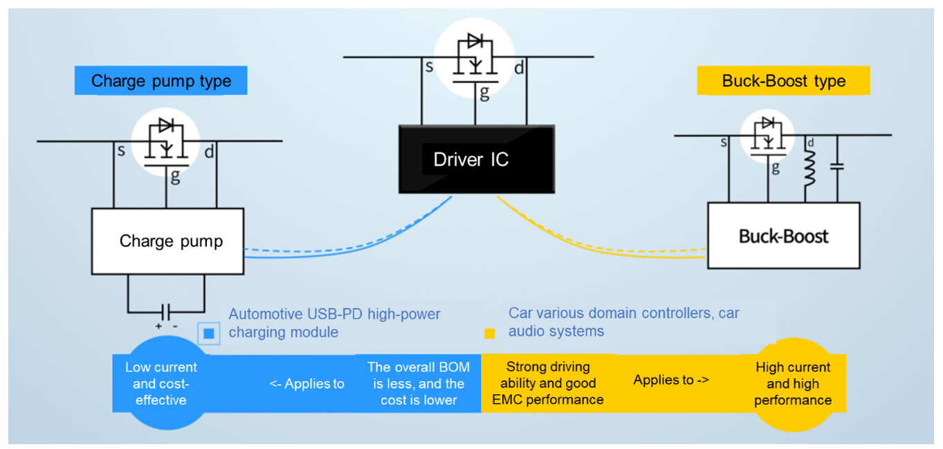
Figure 1: Charge Pump and Buck-Boost Schemes
Working Principles of the Driver IC
Figure 2 shows the simple working principle of the N-channel MOSFET driver with a charge pump topology.
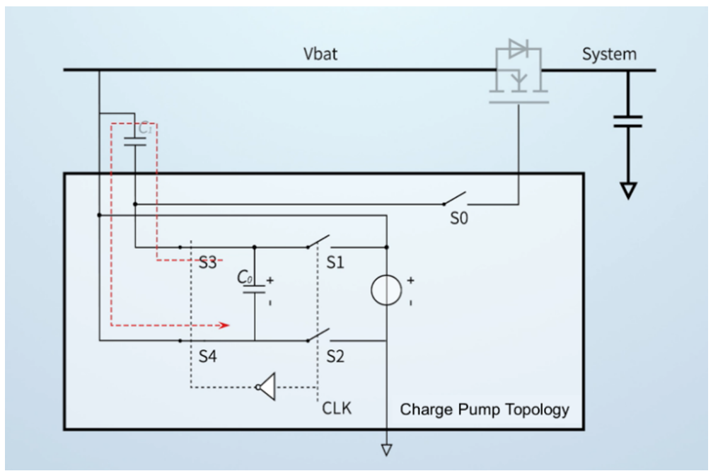
Figure 2: Working Principle of Charge Pump Topology
The CLK cycle is as follows:
- S1 and S2 turn on
- C0 is charged by the internal voltage source relative to ground
- S3 and S4 turn on
- C1 is charged by the voltage on C0
C0 is a small capacitor with fast charging and discharging speed. C1 is a large capacitor with a high load capacity. Therefore, by frequently switching S1 and S2 (as well as S3 and S4), the charge on C0 can be continuously transferred to C1, while the negative end of C1 is connected to the battery voltage (VBATT). As a result, the N-channel MOSFET is driven by a voltage that exceeds VBATT.
Figure 3 shows the simple working principle of the N-channel MOSFET driver with a buck-boost topology.

Figure 3: Working Principle of Buck-Boost Topology
The buck-boost topology places the power MOSFET on the low side. When S_BAT is on, VIN charges the inductor, and the inductor’s voltage is negative. When S_BAT is off, the inductor releases energy through the diode, and the inductor voltage is positive to charge C1. This scheme generates a voltage exceeding VBATT on C1, which then drives the N-channel MOSFET’s gate.
Related Content
-
VIDEO

MPSafe™ Automotive Functional Safety
Introducing our ISO 26262 compliant functional safety product development process
-
WEBINAR

From Cold Crank to Load Dump - A Primer on Automotive Transients
Understand automotive transients occuring in a 12V vehicle system
-
LANDING PAGE

EMC Testing Labs
EMC testing facilities
-
PRODUCT

MPQ5850-AEC1
36V, smart diode controller with reverse protection, AEC-Q100 qualified
Advantages of Buck-Boost Driver IC
Using a buck-boost driver IC in a reverse polarity protection driver IC has two important advantages: it enhances driver current capability and improves EMC performance.
Driver Current Capability
The buck-boost topology offers greater drive current capability and the ability to respond to input disturbances more quickly. Consider the waveforms measured under a 2V, peak-to-peak, 100kHz, superimposed AC input ripple (see Figure 4). This includes the input reverse polarity protection MOSFET’s source pole voltage (pink), the drain pole voltage passing through the reverse polarity protection MOSFET (light blue), the MOSFET driving VGS (red), and the load current (green).
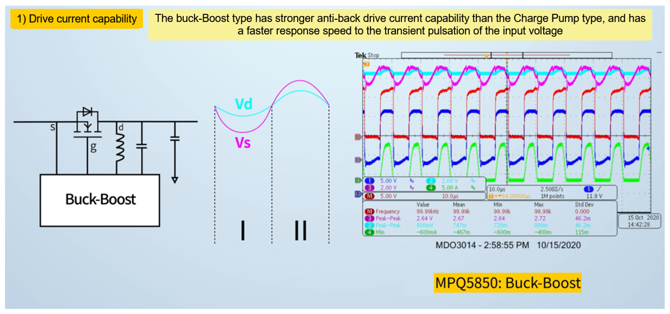
Figure 4: Waveforms of Buck-Boost Topology (Superimposed AC Ripple Pulse = 100kHz, Peak-to-Peak Value = 2V)
The waveforms show that the driver IC monitors the drain and source of the N-channel MOSFET in real time. In this scenario, VIN is consistent with the source voltage (VS), and the system voltage is consistent with the drain voltage (VD).
If VS is below VD, then VIN is below the system voltage, and the MOSFET driver turns off. The body diode uses the reverse polarity protection function to prevent the capacitor current from flowing back. If VS exceeds VD, then VIN exceeds the system voltage, and the MOSFET driver turns on. This prevents the body diode from conducting, which impacts efficiency.
In comparison, when the charge pump reverse polarity protection driver is used, the weak driving current capability tends to cause abnormal gate driver pulse loss or unintended turn-on pulses as VIN fluctuates rapidly.
Consider the waveforms measured using a charge pump reverse polarity protection circuit (see Figure 5). This includes the reverse polarity protection MOSFET’s input source pole voltage (yellow), output drain pole voltage (red), driving VGS (green), and the load current (blue).
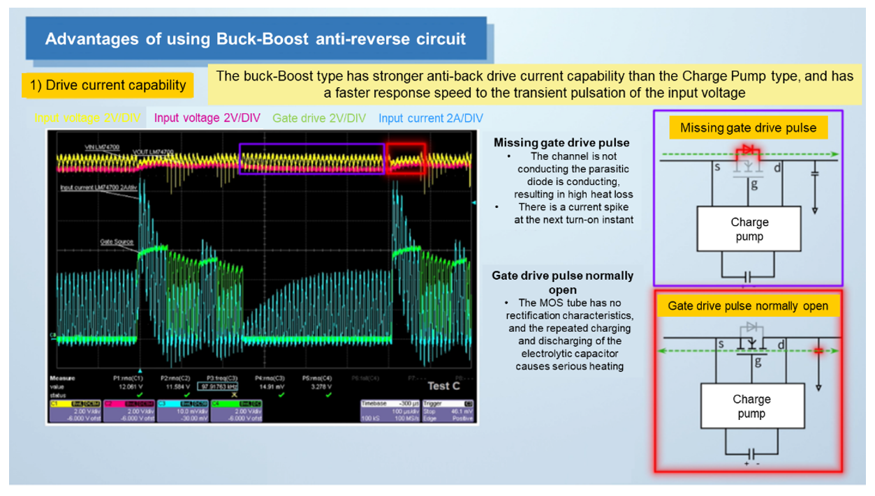
Figure 5: Waveforms of Charge Pump Topology
When the gate driver pulse is lost, the MOSFET is not driven. Meanwhile, the body diode is on, and there is considerable heat loss. At the turn-on moment, there is a large charging current spike.
When the gate driver pulse is on, the MOSFET is typically on. Meanwhile, the electrolytic capacitor is repeatedly charged and discharged, which results in significant heat generation.
Improved EMC Performance
The buck-boost topology also improves EMC performance. Although the charge pump has no inductance, it is a capacitive switching power supply that requires an extremely high operating frequency due to its low efficiency. In general, the integrated capacitance is small (within the pF range), while the external capacitance is large (within the µF range). As a result, the charge pump’s switching frequency (fSW) exceeds 10MHz. This high frequency can cause EMI issues.
Using a buck-boost driver IC improves efficiency. By adopting fixed-peak current control, a lighter load corresponds to a lower fSW. Therefore, the buck-boost topology improves EMC performance (see Figure 6).
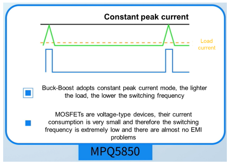
Figure 6: Constant Peak Current of Buck-Boost Topology
Introducing the MPQ5850-AEC1
The MPQ5850-AEC1 is a smart diode controller that achieves reverse input protection by driving an external N-channel MOSFET to replace a Schottky diode. It is well-suited for automotive cold-crank conditions, and is available in a TSOT23-8 package.
Figure 7 compares the EMC performance of the charge pump topology and the MPQ5850-AEC1, which is a buck-boost topology. While the charge pump topology could experience EMC issues, the MPQ5850-AEC1 passes the national standard level 5 test.
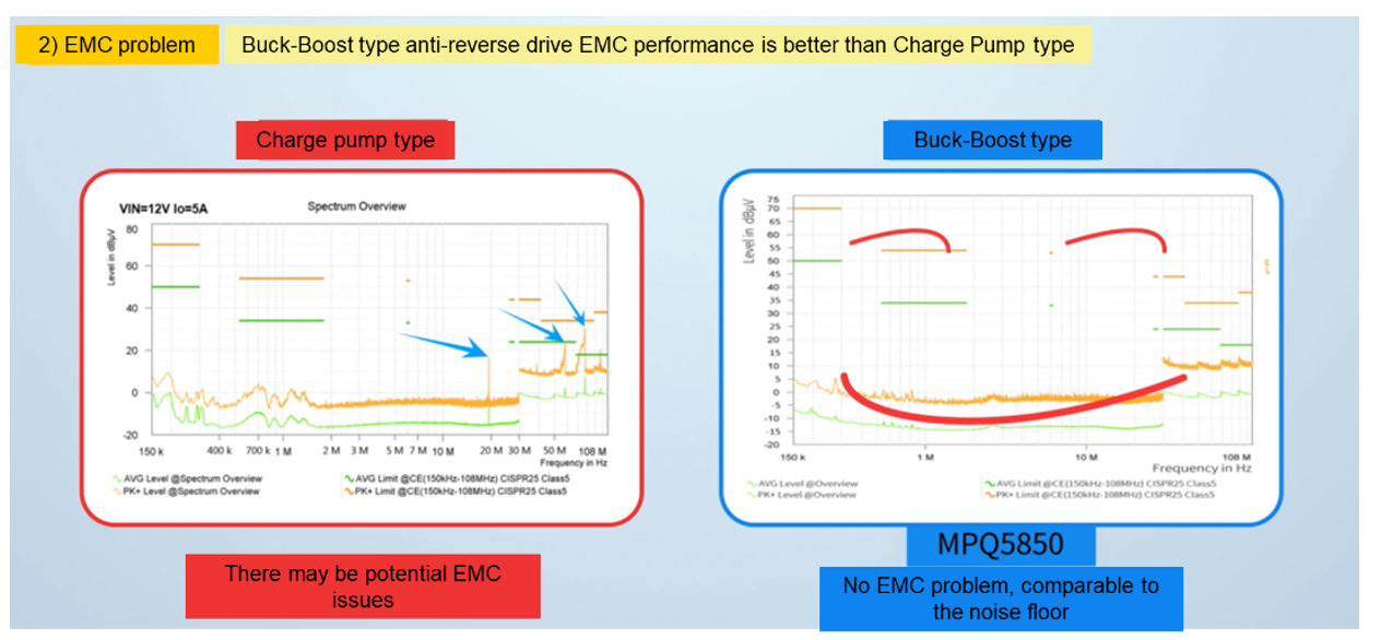
Figure 7: Charge Pump Topology vs. MPQ5850-AEC1
Conclusion
To pass the various test standards for pulse interferences, it is important to achieve an optimal reverse polarity protection circuit design. Compared to the traditional P-channel MOSFET circuit, the N-channel MOSFET circuit improves driver current capability and EMC performance. In particular, the MPQ5850-AEC1 provides reverse input protection and passes the national EMC standards. For more details, explore MPS’s
_______________________
Did you find this interesting? Get valuable resources straight to your inbox - sent out once per month!
Technical Forum
 Latest activity 3 hours ago
 2 Comments
Latest activity a day ago
2 Comments
Latest activity 2 weeks ago
3 Comments
2 Comments
Latest activity a day ago
2 Comments
Latest activity 2 weeks ago
3 Comments
Log in to your account
Create New Account