Designing a Power Tree for an Automotive SoC

Get valuable resources straight to your inbox - sent out once per month
We value your privacy
Introduction
Advanced driver assistance systems (ADAS) and infotainment system-on-chips (SoCs) are offering increasingly higher computing power, which in turn results in higher power demands. An SoC can require more than 10 different power rails, with currents ranging from hundreds of amperes (A) to a few mA. Crafting an optimal power tree for these applications is not a trivial task. This article will discuss how to design an optimal power architecture for an automotive SoC. It particular, it will focus on the pre-regulator design.
Challenges for Automotive Batteries
A 12V battery bus in an automotive environment can experience various stressors, such as transient over-voltage (OV) and under-voltage (UV) conditions that occur during car operation. Due to this, most DC/DC integrated circuits (ICs) that are designed to operate from a PC’s 12V bus are not well-suited for automotive applications. A pre-regulator is required to prepare the field for the low-voltage DC/DC ICs. This pre-regulator should generate a clean bus (typically 5V or 3.3V) from which the core VR and the other converters operate.
System-On-Chip (SoC) Power Requirements
In the early stages of development, the SoC power requirements typically provide each rail’s voltage and current ratings, as well as the expected transient currents that the system must be prepared to support. It is the power architect’s job to translate this information into a comprehensible, high-level diagram from which to start the hardware design. Table 1 shows an example of SoC power requirements.
Table 1: SoC Power Requirements
| Rail Name | Voltage (V) | Current (C) | Transient Load (A) | Slew Rate (A/µs) | Voltage Tolerance (1)(%) | Notes |
| VDD_CORE | 0.85 | 60 | 40 | 40 | 3 | |
| 1V8_GPIO | 1.8 | 5 | 2.5 | 2.5 | 5 | |
| 3V3_GPIO | 3.3 | 5 | 2.5 | 2.5 | 5 | |
| 1V8_analog | 1.8 | 1.5 | 0.75 | 0.75 | 5 | From a low-noise DC/DC converter |
| DDR_VDD | 1.05 | 6 | 3 | 3 | 3 | |
| DDR_VDDQ | 0.6 | 6 | 3 | 3 | 5 | |
| PCIe | 0.85 | 1.5 | 0.75 | 0.75 | 5 | From a low-noise DC/DC converter |
| MIPI | 0.75 | 1.5 | 0.75 | 0.75 | 5 | From a low-noise DC/DC converter |
Note:
1) The voltage tolerance includes the converter's DC accuracy, load transient response, and IR drop.
Figure 1 shows the power tree that can be formed with the SoC power requirements.
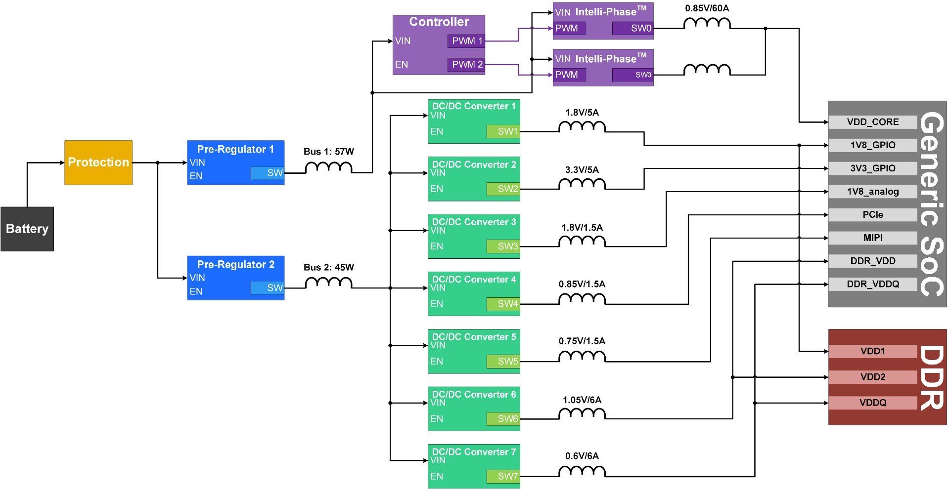
Figure 1: Power Tree
Note that there are two pre-regulators to limit the output power for each converter to about 50W. By implementing two pre-regulators, designers can have more options for IC selection.
Selecting the Pre-Regulator Topology
The first step when designing the pre-regulator is to determine its topology. Depending on the required operating conditions, this regulator can be a buck converter, buck-boost converter, or a combination of buck and boost converters.
If the system must operate during a warm-crank event, but it can turn off briefly during a harsher cold-crank event, it is recommended to select a buck converter topology for improved cost and efficiency. If any circuit needs a voltage exceeding 5V during the warm-crank event, a post-boost converter can be added to ensure that the circuit is supplied with the required voltage. Otherwise, if the circuit must operate under severe cold-crank event as well, choose a buck-boost converter to guarantee that the system operates under all potential conditions. Note that a buck-boost converter is typically more expensive and less efficient has than a simpler buck converter. For this design example, a buck converter was selected.
Related Content
-
REFERENCE DESIGN
Domain Control Module
Automotive power stage for ADAS applications
-
VIDEO
Automotive-Grade Ideal Diode Controller with Reverse Polarity Protection
Smart ideal diode controller offers robust protection for automotive electronics
-
WEBINAR

On-Demand: From Cold Crank to Load Dump
A primer on automotive transients
-
ARTICLE
Developing a Smart Cockpit Solution with MPS and Semidrive
Discover the wide array of features in a smart car’s cockpit
Setting the Bus Voltage
Once the topology is selected, the designer must consider the bus voltage. This bus voltage — typically 3.3V or 5V — supplies all downstream converters. Most low-current DC/DC ICs can operate from up to 5.5V, so either voltage would work. However, solutions with a controller and an Intelli-PhaseTM converter must operate from a ≥5V bus.
The bus voltage is typically selected to optimize cost, as stepping down directly to 3.3V can sometimes reduce the number of required converters, but it also requires a higher output current than when the voltage is converted to 5V.
Each pre-regulator’s power rating is the sum of its downstream converters’ output power when the efficiency coefficient is applied. For simplicity, an 89% efficiency can be assumed for all converters. The power for pre-regulator 1 (PPRE-REG1) can be calculated with Equation (1):
$$P_{PRE-REG1} = \frac {V \times I}{η} = \frac {0.85 \times 60}{0.89} = 57.3W$$The power for power regulator 2 (PPRE-REG2) can be estimated with Equation (2):
$$P_{PRE-REG2} = \frac {\sum_{1} ^{7}V_n \times l_n} {η} = \frac {1.8 \times 5+3.3 \times 5+1.8 \times 1.5+0.85 \times 1.5+0.75 \times 1.5+1.05 \times 6+0.6 \times 6}{0.89} = 45.5W$$Then calculate the output current for each pre-regulator. Calculate pre-regulator 1’s output current (IPRE-REG1_5V) with Equation (3):
$$I_{PRE-REG1\_5V} = \frac {P}{V} = \frac {57.3}{5} = 11.5A$$For pre-regulator 2, estimate the output current using both for the 3.3V bus voltage option (IPRE-REG2_3.3V) using Equation (4):
$$I_{PRE-REG2\_3.3V} = \frac {P}{V} = \frac {45.5}{3.3} = 13.8A$$For pre-regulator 2, estimate the output current using both for the 3.3V bus voltage option (IPRE-REG2_5V) using Equation (5):
$$I_{PRE-REG2\_5} = \frac {P}{V} = \frac {45.5}{5} = 9.1A$$Since this system’s power rating is high, a 5V bus voltage allows for a lower output current than a 3.3V bus voltage. It is recommended to choose a 5V bus voltage so that designers can select a less complex DC/DC converter.
Selecting the IC
Once the topology and output load have been determined, the designer should select the pre-regulator IC. This IC must support a 42V input voltage for load dump conditions, and also be able to operate down to 6V during warm-crank conditions. In addition, the output load capability should be ≥11.5A, or two parts should be able to operate in parallel up to that current. Both pre-regulators can use the same IC since the power level is similar.
The MPQ4360-AEC1 is a synchronous buck converter with a current rating of 6A, and it can operate in a multi-phase configuration to achieve 12A of output current. The interleaved multi-phase operation reduces the electromagnetic emissions and allows for smaller components, which provides the benefit of a smaller PCB layout compared to a solution using a controller and discrete FETs. This device also has a very low 22µA quiescent current (IQ), which makes it well-suited for automotive applications. Figure 2 shows two MPQ4360-AEC1s operating in parallel.
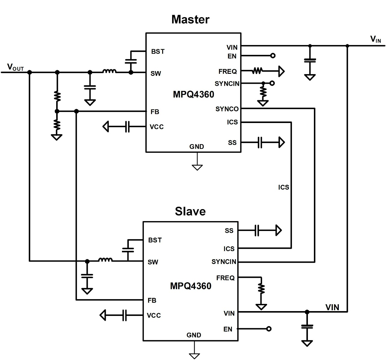
Figure 2: Dual-Phase MPQ4360-AEC1 Schematic
Figure 3 shows an example of the PCB layout for the MPQ4360-AEC1 in dual-phase operation. The approximated solution area is 750mm2.
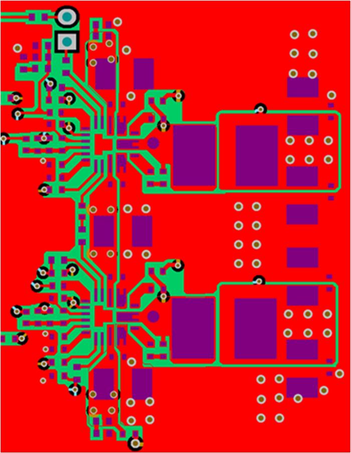
Figure 3: PCB Layout of Dual-Phase MPQ4360-AEC1 Devices
System Protections
The battery bus can experience a hazardous reverse supply voltage. If the system is not protected in this scenario, all the devices can be damaged. To prevent reverse current flow, a diode is typically added to the input line. However, diodes have a forward voltage (VF). As current flows through the diode during normal operation, VF creates a power loss.
The designed SoC system has a power rating of >100W; for a 12V battery, this translates to an input current that can exceed 8A. 8A is too large for a simple diode — and even when using a Schottky diode with a VF of 0.3V, the power loss would exceed 2.4W. A standard alternative is to use a P-channel MOSFET to block the reverse current, but these MOSFETs may not be able to protect the IC from high-frequency AC currents in a sufficient timeframe.
The MPQ5850-AEC1 is an ideal diode controller that can protect the system from reverse current flow. The MPQ5850-AEC1 controls an N-channel MOSFET with a strong gate driving capability to quickly block any reverse current flow (see Figure 4). This provides reverse current protection with minimal power loss.
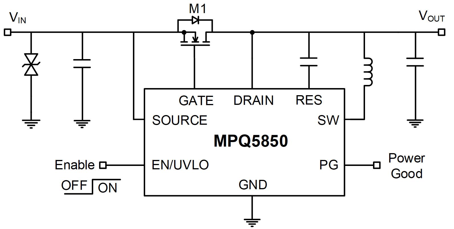
Figure 4: MPQ5850-AEC1 Ideal Diode Controller
When the pre-regulator and protection device are selected, the power tree can be updated to reflect the selected parts (see Figure 5).
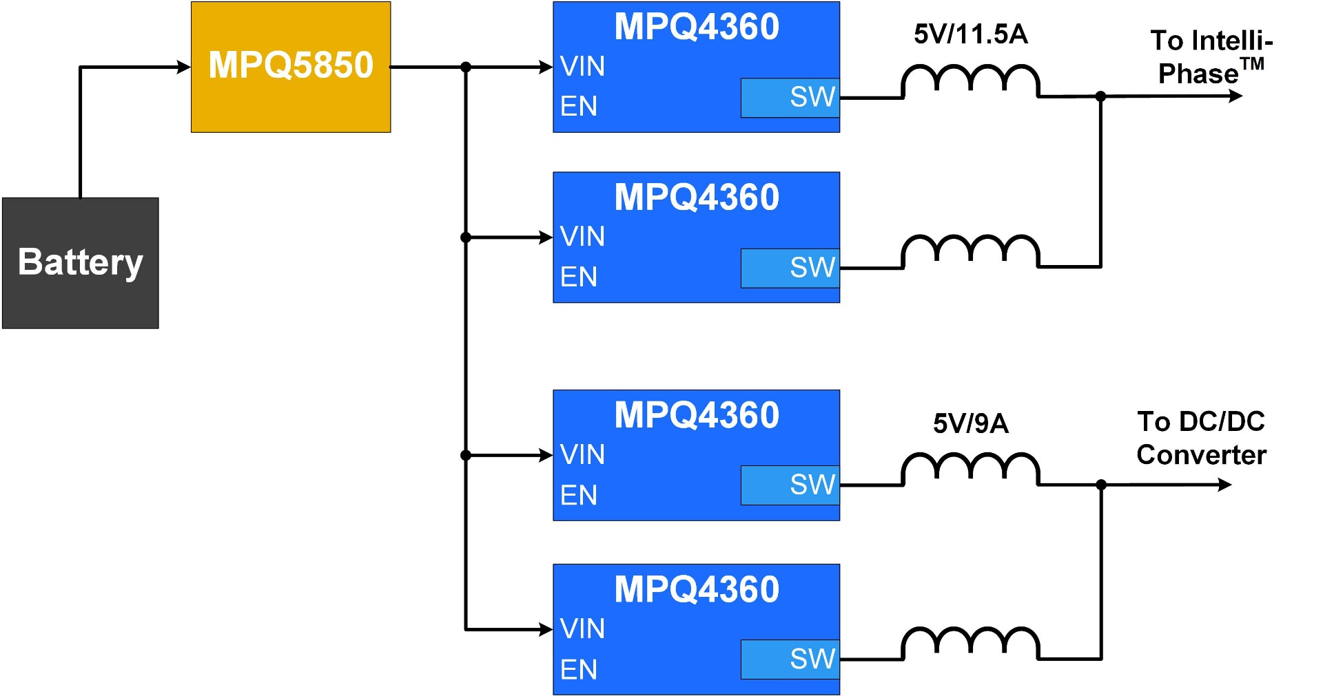
Figure 5: Final Pre-Regulator and Protection Power Tree
Conclusion
Selecting the correct pre-regulator for an ADAS system is not an easy task. Using an IC that allows its output to be paralleled in a multi-phase topology makes this design more straightforward. The scalable solution using the MPQ4360-AEC1 and MPQ5850-AEC1 allows each rail to meet its required output current in a small area, while reducing BOM cost.
For additional reading, refer to the following article to learn more about automotive transients.
_______________________
Did you find this interesting? Get valuable resources straight to your inbox - sent out once per month!
Technical Forum
 Latest activity a week ago
 3 Comments
Latest activity 3 weeks ago
2 Comments
Latest activity 4 weeks ago
4 Comments
3 Comments
Latest activity 3 weeks ago
2 Comments
Latest activity 4 weeks ago
4 Comments
Log in to your account
Create New Account