MP2731 1-Cell Solar MPPT Charger Reference Design
DOWNLOAD THE FULL REFERENCE DESIGN

Get valuable resources straight to your inbox - sent out once per month
We value your privacy
MP2731 – Single-Cell Switching Charger with MC96F1206
In an era characterized by the internet of things (IoT), more connectivity means more outdoor devices are now battery-powered and constantly communicating. In particular, there is an increasing number of outdoor devices being powered through solar panels. This reference design is for maximum power point tracking (MPPT) in outdoor designs with a solar panel. It illustrates design tips for a solar panel charger with a Lithium-ion battery, and is suitable for applications such as outdoor solar surveillance cameras or outdoor lighting.
This reference design is developed based on the MP2731, a single-cell switching charger IC from MPS, and the MC96F1206 controller (a low-cost 8051 MCU). It is suitable for small and medium solar-powered charging solutions. The MP2731 integrates a VIN connection switcher, an ADC, and a voltage/current-sense circuit, which significantly reduce system size and cost. This reference design uses a perturb-andobserve (P&O) algorithm for MPPT to achieve a minimum 98% tracking accuracy.
MP2731 Features
- Wide 3.7V to 16V Operating Input Range
- Up to 22V Sustainable Input Voltage
- Up to 4.5A Charge Current
- Up to 93% Charge Efficiency in 9V Input 5W System
- Up to 98% MPPT Accuracy
- Low to 41.5μA Battery Current in Standby Mode
- Low to 13μA Battery Current in Shipping Mode
- NVDC PPM to Support System Instant-On and Battery Supplement
- I2C Interface for Flexible System Parameter Setting and Status Reporting
- Robust Charging Protections, including Configurable JEITA and Safety Timer
- Available in a 25mmx25mm Core Circuit Area

Figure 1: Evaluation Board
Applications
- Outdoor Solar Surveillance Cameras
- Outdoor Lighting
- E-Bike Battery Chargers
Solar Charger System Block Diagram
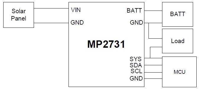
Figure 2: Solar Charger System Block Diagram
Related Solutions
This reference design is based on the following MPS solution:
| MPS Integrated Circuit | Description |
| MP2731 | Single-cell switching charger with I2C control and NVDC PPM |
Solar Charger System Specifications
| Parameter | Specification |
| Input voltage range | 3.7V to 16V |
| System output voltage | Up to $V_{BATT}$ (about 3.6V) + 100mV |
| System output current | Up to 4.5A |
| Charge current | Up to 4.5A |
| Switching frequency | 1350kHz |
| Board form factor | 63mmx63mmx3mm |
Solar Charger System Design
MP2731 Single-Cell Switching Charger
The MP2731 is a 4.5A, highly integrated, switch-mode battery charger with NVDC power path management for a single-cell Li-ion or Li-polymer battery.
Inductor Selection
Inductor selection is a tradeoff between cost, size, and efficiency. From a practical standpoint, the inductor ripple current should not exceed 30% of the maximum load current under worst-case conditions. If the MP2731 operates with a 5V input voltage, the maximum inductor current ripple occurs after precharge, and when constant current (CC) charge begins. The inductance can be estimated with Equation (1):
$$ L= \frac { V_{IN} - V_{SYS} }{ \Delta I_{L\_MAX}} \frac {V_{SYS}}{V_{IN}\, x \, f_{SW}(MHz)}(\mu H)$$Where $V_{IN}$ is the input voltage, $V_{SYS}$ is the system voltage, $f_{SW}$ is the switching frequency, and $\Delta I_{L\_MAX}$ is the maximum inductor ripple current, which is about 30% of the CC charge current.
The peak current can be calculated with Equation (2):
$$I_{PEAK} = I_{LOAD(MAX)}\, x\, \left(1+ \frac{\%ripple}{2}\right)(A)$$The MP2731 has a maximum charge current of 4.5A, but the actual charge current cannot reach this value for the input current limit. For most applications, the maximum inductor current ripple is set to 0.5A with a 5V input voltage, so the inductor is $1.5\mu H$. For small applications, select a $1.0 \mu H$ inductor with a low DC resistance to optimize efficiency.
System Capacitor Selection
To ignore the ESR of the output capacitor, use a small ceramic capacitor with a lower ESR. The output voltage ripple can then be estimated with Equation (3):
$$\Delta r = \frac{\Delta V_{SYS}}{V_{SYS}} = \frac {1-{V_{SYS}\over V_{IN}}}{8\,x\,C_{SYS}\,x\,{f_{SW}}^2\,x\,L} \%$$To guarantee the ±0.5% system voltage accuracy, the maximum output voltage ripple must not exceed 0.5% (e.g. 0.1%). The maximum output voltage ripple occurs at the minimum system voltage and the maximum input voltage.
If $V_{IN} = 5V, V_{SYS} = 3.7V, L = 1\mu H, f_{SW} = 1.35MHz$, and $\Delta r = 0.1%,$ the output capacitor can be calculated with Equation (4):
$$C_{SYS} = \frac {1-{V_{SYS}\over V_{IN}}}{8\,x\,{f_{SW}}^2\,x\,L\,x\,\Delta r}$$In this example, choose a $22\mu F$ ceramic capacitor.
MPPT Theory
The output power from a solar panel is determined by several factors: the irradiance level, the operating voltage and current of the panel, and the load. There is a maximum power point where the solar panel outputs optimal power to the system (see Figure 3). Maximum power point tracking techniques, such as perturb-and-observe (P&O) or incremental conductance methods, ensure that the solar panels operate at MPPT under conditions where the irradiance changes.
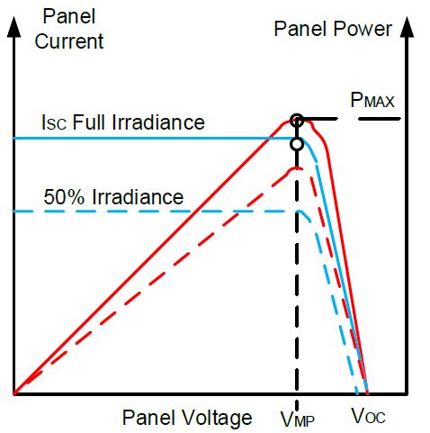
Figure 3: Solar Panel P-V and I-V Curve
In the power-based P&O MPPT algorithm, the power-to-voltage derivative $(dP_O/dV_O)$ of a solar panel is used as a tracking parameter. Calculate when MPP is reached using Equation (5):
$$\frac{dP_O}{dV_O}=0$$Where $P_O$ is the solar panel output power, and $V_O$ is the solar panel output voltage.
MPPT Software Implementation
The P&O MPPT algorithm is implemented in a 20-pin, 8-bit MC96F1206 MCU from ABOV Semiconductor. To communicate with the MP2731, the I2C peripherals in the MCU are activated. Figure 4 shows the system-level software flow.

Figure 4: System-Level Software Flowchart
Note:
Before updating I_OFFSET, turn off other devices connected at the MP2731’s SYS pin to ensure that I_OFFSET is calibrated correctly
The MCU enters sleep mode if VIN experiences an input power failure. If VIN is sufficient, the INT interrupt signal is sent to wake up the MCU. Then the MCU reads the MP2731 registers and initiates the registers (see Table 1).
| Register Address | Value (Hex) | Value (Bin) | Description |
| 0x00 | 0x7F | 0111 1111 | Sets the input current limit to 3.25A (maximum). |
| 0x02 | 0xDC | 1101 1100 | Automatic input current optimization is disabled. |
| 0x03 | 0x50 | 0101 0000 | ADC continuous conversion is enabled. |
| 0x08 | 0x84 | 1000 0100 | Termination is enabled, and WTD and safety time are disabled. |
| 0x0B | 0xC0 | 1100 0000 | USB detection is disabled. |
By setting the input current limit to its maximum value, the panel voltage is controlled only by the input voltage limit loop. By adjusting the input voltage limit loop reference, the PV panel’s voltage can be adjusted. After initializing the MP2731, read the ADC initial value, and then enable charging.
If VIN_STAT is not equal to 1, increase VIN_REG by one unit, and then continue to go back to the previous VIN_STAT value. If VIN_REG reaches its maximum limit and VIN_STAT is still is not equal to 1, gradually decrease the charging current and return to the previous VIN_STAT value.
If VIN_REG set has reached its limit, the ICC set has a minimum at the same time. However, if VIN_STAT still is not equal to 1, the MCU goes into sleep mode. Meanwhile, the MP2731’s charging is disabled until the INT interrupt wakes the MCU.
If the PV panel is partially covered and a local MPP can be tracked using a conventional P&O MPPT algorithm, then the MCU initiates a scan every time the input voltage flag changes. To find the optimal power point, the MCU adjusts the input regulation voltage reference of the MP2731 with a 100mV step from 50% of the panel’s open-circuit voltage (VOC) to 80% of VOC.
After the initial scan, the PV panel operates at the maximum power point. To continue tracking the optimal point under varying load and irradiance conditions, the P&O algorithm runs every 256ms on the MCU (see Figure 5).
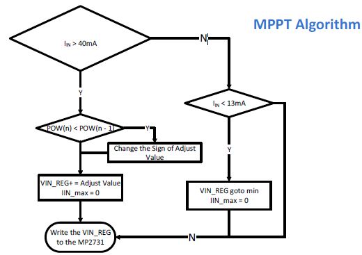
Figure 5: P&O MPPT Algorithm
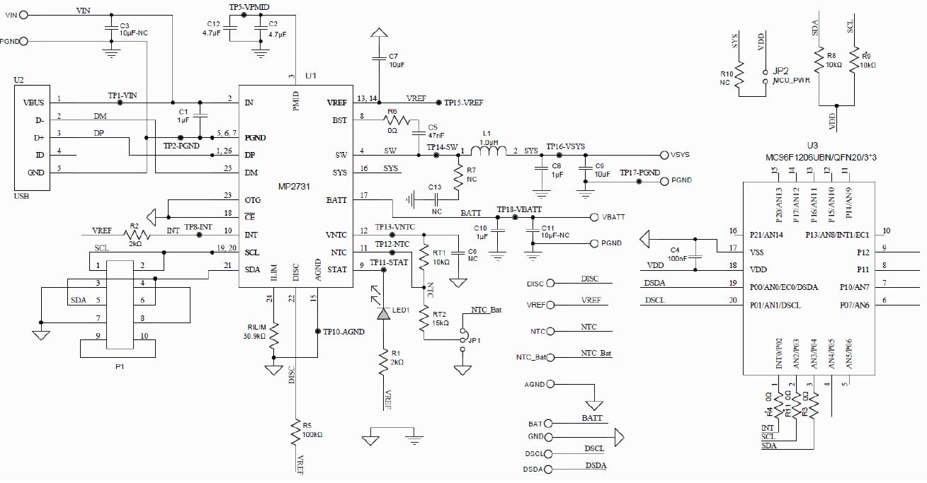
Figure 6: Battery Charger with MPPT Schematic
BOM
| Qty | Ref | Value | Description | Package | Manufacturer | Manufacturer P/N |
| 1 | C1 | 1µF | Ceramic capacitor, 25V, X7R | 0603 | Murata | GRM188R71E105KA12D |
| 1 | C2 | 10µF | Ceramic capacitor, 50V, X5R | 1206 | Murata | GRM31CR61H106KA12L |
| 1 | C4 | 100nF | Ceramic capacitor, 25V, X5R | 1206 | Murata | GCM188R71C104KA37D |
| 1 | C5 | 47nF | Ceramic capacitor, 25V, X5R | 0603 | Murata | GRM188R71H473KA61D |
| 1 | C7 | 10µF | Ceramic capacitor, 16V, X5R | 0603 | Murata | GRM188R61C106KAALD |
| 2 | C9, C11 | 22µF | Ceramic capacitor, 10V, X7R | 1206 | Murata | GRM31CR71A226KE15L |
| 1 | C3 | NC | Ceramic capacitor | 1206 | ||
| 1 | C12 | NC | Ceramic capacitor | 0805 | ||
| 4 | C6, C8, C10, C13 | NC | Ceramic capacitor | 0603 | ||
| 1 | L1 | 1µH | Inductor, 1µH, 21mΩ, 7A | SMD | Cyntec | HTEP32251B-1R0MIR-89 |
| 1 | LED1 | Red LED | 0805 | Bright LED | BL-HUF35A-TRB | |
| 2 | R1, R2 | 2kΩ | Film resistor, 1% | 0603 | Yageo | RC0603FR-072KL |
| 1 | RLIM | 1kΩ | Film resistor, 1% | 0603 | Yageo | RC0603FR-071KL |
| 4 | RT1, RT2, R8, R9 | 10kΩ | Film resistor, 1% | 0603 | Yageo | RC0603FR-0710KL |
| 5 | R3, R4, R6, R10, R11 | 0Ω | Film resistor, 1% | 0603 | Yageo | RC0603FR-070RL |
| 1 | R5 | 100kΩ | Film resistor, 5% | 0603 | Yageo | RC0603JR-07100KL |
| 1 | R7 | NC | Film resistor | 0603 | ||
| 2 | JP1, JP2 | 2.54mm connector | ||||
| 2 | JP1, JP2 | 2.54mm short | ||||
| 1 | P1 | Header, 5-pin, dual row | ||||
| 10 | GND, DISC, NTC, INT, VREF, NTC_BAT, BATT, GND, DSCL, DSDA | 2.54mm connector | ||||
| 6 | VIN, PGND, VBATT, PGND, PGND, VSYS | 2mm pin | ||||
| 11 | GND, VPMID, DP, DM, VIN, VBATT, VSYS, GND, SW, BST, STAT | Test point | ||||
| 1 | U1 | MP273 1 | I2C-controlled switching charger with NVDC power path and USB OTG | QFN-26 (3.5mmx 3.5mm) | MPS | MP2731GQC-0001 |
| 1 | U2 | NC | Micro-B USB receptacle | 7.5mmx 2.45mmx5mm | ||
| 1 | U3 | MCU | QFN-20 (3mmx 3mm) | ABOV | MC96F1206USBN |
PCB layout is critical for stable operations. For the best results when designing the general switching design, refer to Figure 7 and follow the guidelines below:
PCB Layout
- Route the power stage adjacent to the grounds.
- Minimize the high-side switching node (SW, inductor) trace lengths in both the high-current paths and the current-sense resistor trace.
- Keep the switching node short and route it away from all small control signals, especially the feedback network.
- Place the input capacitor as close as possible to the PMID and PGND pins.
- Place the output inductor close to the IC, and connect the output capacitor between the inductor and PGND of the IC.
- For high-current applications, the pins for the power pads (IN, SW, SYS, BATT, and PGND) should be connected to as much copper in the board as possible. This improves thermal performance because the board conducts heat away from the IC.
- Connect a ground plane directly to the return of all components through via holes.
- If possible, place via holes inside the PGND pads for the IC.
- It is recommended to use a star ground design approach to keep circuit block currents isolated (highpower/ low-power, small-signal), which reduces noise coupling and ground-bounce issues. A single ground plane for this design gives good results. With this small layout and a single ground plane, there is no ground bounce issue, and having the components segregated minimizes coupling between signals and stability requirements.
- Pull the connect wire from the MCU (I2C) far from the SW mode and copper areas.
- Place SCL and SDA in close parallel.
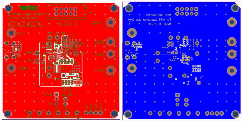
Figure 7: Recommended PCB Layout Top Layer (Red) and Bottom Layer (Blue)
Test Results
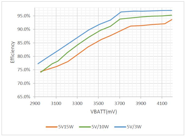
Figure 8: Charging Efficiency (5V Panels with Different Power)

Figure 9: Charging Efficiency (9V Panels with Different Power)

Figure 10: Charge Efficiency (12V Panels with Different Power)
Time Domain Waveforms

Figure 11: MPPT Process for PV Panel from Start-Up to Steady State

Figure 13: Tracking Performance for Panel when Partially Shaded and when Shade Removed (5V Panel)

Figure 15: Tracking Performance for Solar Irradiance Changing (5V Panel)

Figure 12: MPPT Behavior during Charging Profile

Figure 14: Tracking Performance for Panel when Partially Shaded and when Shade Removed (8V Panel)

Figure 16: Tracking Performance for Solar Irradiance Changing (8V Panel)
Log in to your account
Create New Account