AN183 - Designing an Isolated Gate Driver Power Supply with LLC Topology

Get valuable resources straight to your inbox - sent out once per month
We value your privacy
ABSTRACT
Unregulated flyback converters and push-pull converters are typically used for isolated gate driver power supply applications, which require a tightly coupled transformer to reduce power loss caused by the inductance leakage. Modern high-power systems often have a higher bus voltage (VBUS) and dV/dt at the switching nodes. A higher isolation voltage (VISOLATION) rating and lower interwinding capacitance are required for transformer design; however, these cannot be achieved on a tightly coupled transformer.
Resonant topology is an ideal solution for this issue. It utilizes the inductance leakage, which allows for a loosely coupled transformer. The advantages of resonant topology include reduced interwinding capacitance and transformer size, as well as high efficiency and improved load regulation.
AN183 provides a step-by-step design guide for a low-cost LLC converter. This converter is designed for isolated gate drivers in IGBT and Si/SiC MOSFET devices. The design is ideal for automotive and industrial applications, including electric vehicle motor drivers, onboard chargers, and grid-tied inverters.
INTRODUCTION
A half-bridge primary-side MOSFET and half-bridge secondary-side rectifier are preferred for low-power applications, as they require fewer switches and diodes. The LLC converter design employs a transformer (T1), magnetizing inductance (Lm), and inductance leakage (Ll1, Ll2). The resonant capacitor (Cr) and the inductance leakage form an LC resonant tank. Selecting a switching frequency (fSW) similar to the resonant tank’s frequency (fr) keeps the resonant tank impedance at about 0Ω. If the LLC converter has a conversion ratio equal to the transformer turns ratio (1:N of T1), then the LLC converter can operate as a DC transformer. Empirically, this statement holds true so long as Lm > 10 x Ll1. In cases where Lm is comparable to Ll1, the conversion ratio exceeds the transformer turns ratio (N) and becomes $$N(1+ \frac{L_{l1}}{L_M})$$
Figure 1 shows an LLC topology scheme.

Figure 1: LLC Topology Scheme
1. MPS Gate Drive Power Supply Solution Using LLC Topology
The LLC converter design employs the MPQ18913 as a half-bridge transformer driver. It features a high fSW and a wide input voltage (VIN) range for system design flexibility. Figure 2 shows the gate driver power supply design schematic for a SiC device.
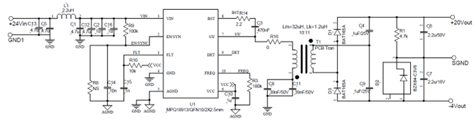
Figure 2: Gate Driver Power Supply Design Schematic for a SiC Device =
A Zener diode splits the output voltage (VOUT) into two rails, which can be used for suitable for a IGBT or SiC driver.
Table 1 shows the component selection and equations for the LLC converter using the MPQ18913.
Table 1: Design Equations and Component Selection for the LLC Converter
| Parameter | Equation and Descrption | Notes |
| Switching frequency (fsw) | $$f_{sw} = \begin{cases}
0.5\, \text{MHz} - 0.75\, \text{MHz}, & P_{out} < 6\,W \\
0.75\, \text{MHz} - 2\, \text{MHz}, & P_{out} < 3\,W \\
1.5\, \text{MHz} - 5\, \text{MHz}, & P_{out} < 2\,W
\end{cases}$$
A higher fSW has larger transformer winding AC resistance, which limits the output power. |
MPQ18913 fSW = 5MHz |
| Transformer magnifying inductance (Lm) | $$\text{L}_m \le \frac{\text{Dead Time}}{8 \times \text{Coss} \times f_{sw}} = \frac{25\,ns}{8 \times 0.15\,nF \times f_{sw}}$$
This Lm guarantees the zero-voltage switching (ZVS) of the primary switches. |
See the Transformer Design section for more details on the design of T1. |
| Rectification diodes (D1 and D3) | $$I_{PEAK}=\pi \times I_{OUT}$$
Use Schottky diodes to minimize switching losses and achieve ZVS. |
The recommendation of D1 and D3 will be shown in section 3 |
| Output capacitors (C6 and C7) | $$C_6 = C_7 \geq \frac{Q_g}{V_{\text{RIPPLE}}}$$
Where Qg is the gate charger of the powered device (e.g. SiC or IGBT), and VRIPPLE is the maximum voltage ripple. |
If C6 and C7 should be >22µF, then choose the MPQ18913A for the design in place of the MPQ18913. |
| Frequency-setting resistor (R3) | $$R_3 = \frac{100k\Omega}{f_{sw} \text{(MHz)}}$$ | |
| Resonant Capacitor (Cr) | $$C_r = \frac{1}{4 \times \pi^2 \times (2 \times L_{l1}) \times f_{sw}^2}$$ | The inductance leakage (Ll1) is determined after designing the transformer. |
2. Transformer Design
The key specifications of the transformer are magnetizing inductance, power loss, isolation voltage (VISOLATION) rating, and coupling capacitance. There are two types of transformers (toroid and planar) that are recommended due to their ease of design and low coupling capacitance.
2.1. Core Material Selection
To take advantage of the MPQ18913’s high fSW, the core should be able to operate at high frequencies. The core material should have a low relative permeability (between 100 and 1000). Some core material options include P9L (0.5MHz to 1.5MHz, manufactured by Encore), PC50 (1MHz to 2MHz, manufactured by TDK), and 61 material (≥2MHz, manufactured by Fair-Rite).
2.2. Toroid Transformer
To set up the toroid transformer, follow the guidelines below:
1. Select the toroid transformer turns ratio.
At the resonant frequency (fr), the LLC converter voltage gain is equal to the transformer turns ratio (N), which can be calculated with Equation (7):
$$N=\frac{V_{OUT\_MIN}+2V_f+V_{RESISTIVE\_DROP}+V_{HEADROOM}}{V_{IN\_MIN}}$$Where VF is the voltage drop of the rectification diodes (D1 and D3), VRESISTIVE_DROP is the voltage drop across primary-side MOSFETs and the resistance of transformer windings, VOUT_MIN is the lower limit for VOUT, VIN_MIN is the lowest VIN, and VHEADROOM is the VOUT drop caused by the dummy load (e.g. an R1 power loss or an extra resistive load connected between +20VOUT and -4VOUT).
Note that VRESISTIVE_DROP is proportional to the load current (ILOAD), and is critical to the load regulation of the gate driver’s power supply. For load regulation, a minimum number of turns (N) are recommended to reduce the resistance of the transformer windings.
(2VF + VRESISTIVE_DROP) can be estimated with Equation (8):
$$2V_F+V_{RESISTIVE\_DROP}=(4N+4) \times I_{LOAD}$$Figure 3 shows a toroid transformer.
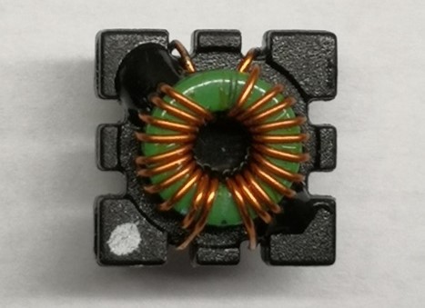
Figure 3: Toroid Transformer
2. Select the window size.
The window size of the toroid transformer requires careful selection to fit the windings. Given number of turns, the diameter of the magnet wire can be calculated with Equation (9):
$$D_{TOTAL}=D_{CONDUCTOR}+2 \times T_{INSULATION}$$Where DTOTAL is the diameter of the winding wire, DCONDUCTOR is the diameter of conductor, and TINSULATION is the thickness of the insulation layer.
DCONDUCTOR can be four times the skin depth at fSW. TINSULATION is related to the VISOLATION rating. If the required VISOLATION is below 2kV, then choose an enameled wire with a breakdown voltage (VBREAK) that exceeds the transformer’s VISOLATION rating. If the required VISOLATION exceeds 2kV, then double- or triple-insulated wires are recommended. If the turns ratio (N) does not equal 1, then use a thicker insulation layer for the low-voltage side of the windings. The two sides should have a VBREAK equal to double the VISOLATION rating.
Figure 4 shows the geometric structure of a toroid core.
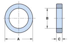
Figure 4: Toroid Core Geometric Structure
The toroid core’s inside diameter (B) must be able to fit the windings. B can be calculated with Equation (10):
$$N_1 \sin^{-1}\frac{D_1}{B-D_1}+N_2 \sin^{-1}\frac{D_2}{B-D_2}\lt\frac{2}{3}\pi$$Where N1 and N2 are the number for turns, and D1 and D2 are the wire diameters.
3. Select the core size based on the inductance per square turn (AL) and the core loss.
AL can be calculated with Equation (11):
$$L_m=N_1^2 \times A_L$$Where Lm is the transformer magnifying inductance, which can be calculated with Equation 2 (see Table 1 on page 4). The other two geometric parameters (A and C) can be selected accordingly with AL.
The maximum flux density (BMAX) can confirm whether the core loss is acceptable. BMAX can be calculated with Equation (12):
$$B_{MAX}=\frac{V_{IN\_MAX}}{4 \times f_{SW} \times N_1 \times (A-B) \times C}$$Consider the core loss density (provided by the core material vendor) at fSW and BMAX. The core loss density should not exceed 150mW/cm3 for thermal performance. If the application requires the density to exceed 150mW/cm3, then select a core that has a larger effective area or more turn windings.
4. Select the transformer bobbin.
Select a transformer bobbin that fits the core and windings. The transformer bobbin size and creepage between the leads of the primary and secondary sides is critical. It is recommended to have a ≥3.5mm creepage for a 3kV VISOLATION rating, and ≥7mm creepage for a 5kV VISOLATION rating.
After the transformer is built, its leakage inductance can be measured by the primary side while the two terminals of the secondary side are shorted. Then the resonant capacitance can be calculated with Equation 6 (see Table 1 on page 4).
2.3 Planar Transformer
To set up the planar transformer, follow the guidelines below:
1. Select the planar transformer turns ratio.
The method to determine the planar transformer turns ratio is the same as the toroid transformer. Follow step 1 in the Toroid Transformer section on page 4 to determine the planar transformer turns ratio.
Figure 5 shows a planar transformer with an ER core.

Figure 5: Planar Transformer with an ER Core
2. Select the window size.
If a 6-layer PCB layout is used, then use the middle layer to form the primary and secondary side as follows:
- Form the primary side by connecting mid-layer 1 and mid-layer 2 in series using coils.
- Form the secondary side by connecting mid-layer 3 and mid-layer 4 in series using coils.
Do not connect coils on the top and bottom layers to avoid masking the core by Hi-pot breakdown.
Figure 6 shows the geometric structure of an ER core.
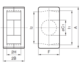
Figure 6: ER Core Geometric Structure
The window size (l1 - C1) can be calculated with Equation (13):
$$\frac{l_1-C_1}{2}\ge \frac{N_X}{2} \times W_{TRACE}+(\frac{N_x}{2}-1) \times W_{CLEARANCE}+2 \times L_{INSULATION}$$Where NX is the number of turns of the primary/secondary side, WTRACE is the PCB trace width (10mil for a 0.25 load on 1oz PCB), WCLEARANCE is the clearance between the two PCB traces (1oz PCB requires a ≥4mil clearance, typically), and LINSULATION is the clearance between the PCB trace and the core.
Then LINSULATION can be calculated with Equation (14):
$$L_{INSULATION}=\frac{V_{ISOLATION}}{2 \times E_b}$$Where Eb is the dielectric strength of the pre-preg material.
The clearance between the primary and secondary sides in all directions can be calculated with Equation (15):
$$T_{INSULATION}=\frac{V_{ISOLATION}}{E_b}$$For typical PCB layouts, the dielectric strength should be 250V/mil.
3. Determine the inductance per square turn (AL).
The optimal AL can be calculated with Equation 11 on page 6 or with Equation 2 (see Table 1 on page 4). If the permeability of the selected core material is high, then the air gap is required to reduce AL. An air-gapped core is shown in Figure 7 shows an ER core with an air gap.
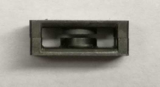
Figure 7: ER Core with an Air Gap
4. Select the core size.
Select the inner height (2H) according to the total PCB thickness . Then select a core that fits the PCB and coils.
BMAX can confirm whether the core loss is acceptable. BMAX can be calculated with Equation (16):
$$B_{MAX}= \frac {V_{IN\_MAX}}{8 \times f_{SW} \times N_1 \times A_e}$$Consider the core loss density (provided by the core material vendor) at fSW and BMAX. The core loss density should not exceed 200mW/cm3 for thermal performance. If the application requires the density to exceed 200mW/cm3, then select a core that has a larger effective area or more turn windings.
After the transformer is built, its leakage inductance can be measured by the primary side while the two terminals of the secondary side are shorted. Then the resonant capacitance can be calculated with Equation 6 (see Table 1 on page 4).
3. Selecting the Rectification Diodes
The diode capacitance (CT) and reverse current (IR) are two significant parameters of the rectification diodes. CT and IR can affect load regulation negatively.
CT is part of the LLC resonant network, and raises the gain of the LLC converter at light loads. A small CT is recommended for improved load regulation.
IR increases as the diode temperature increases. At heavy loads, the temperature of the diodes rise, and IR adds an extra load to the LLC converter. This increases load regulation.
Considering these parameters, it is recommended to use BAT165 (40V, 0.75A, AEC-Q101) or PMEG6010CEJ (60V, 1A, AEC-Q101) for the rectification diodes.
_______________________
Did you find this interesting? Get valuable resources straight to your inbox - sent out once per month!
Technical Forum
 Latest activity 2 years ago
 5 Comments
Latest activity a month ago
7 Comments
Latest activity 3 weeks ago
14 Comments
5 Comments
Latest activity a month ago
7 Comments
Latest activity 3 weeks ago
14 Comments
Log in to your account
Create New Account