Power Supply Design for Car Infotainment Systems (Part II)

Get valuable resources straight to your inbox - sent out once per month
We value your privacy
Introduction
This article is the second part of a two-part series covering power supply design for car infotainment systems. Part I discussed the performance requirements for primary and secondary power supplies in car infotainment systems. Part II addresses challenges regarding camera power supplies and USB charging in car infotainment systems.
Figure 1 shows the car machine’s power architecture, including the camera power supply and USB charging.

Figure 1: Power Architecture of Camera Power Supply and USB Charging
MPS provides solutions that can help designers meet the requirements for surround-view camera power supplies and USB charging applications.
Surround-View Camera Power Supply Solution
There is an emerging demand for modern vehicles to integrate the surround-view camera’s image processing into the vehicle’s main processor. Figure 2 shows that surround-view camera modules, which are typically distributed around the car, transmit data and power to the central processing unit (CPU) in the cab through long coaxial cables.
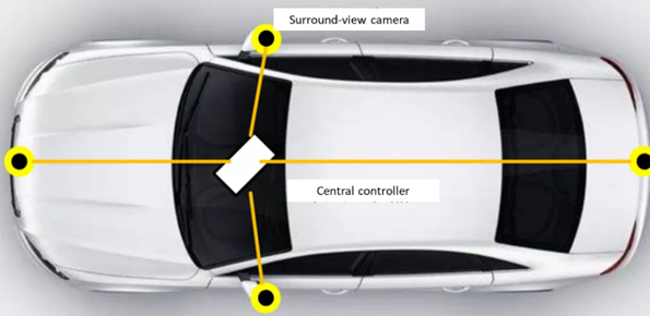
Figure 2: Surround-View Cameras Transmit Data to CPU
In general, the module’s power supply inside the camera is below 5V. When considering the voltage drop across long-distance lines or voltage drops caused by other factors (e.g. cold crank), some car manufacturers have set the power supply to the camera to about 8V to 10V, though this poses challenges for car batteries.
For example, when the car is being tested under cold-crank conditions, the battery voltage can drop to as low as 5V. At the same time, the normal operating voltage range must support a minimum of 9V. For standard step-down DC/DC converters, it can be difficult for the camera supply rail to stay within these conditions. A two-stage power supply architecture (one that bucks first and then boosts) could be used, though this architecture is inefficient and takes up more PCB space.
The MPQ8873-AEC1 is a monolithic, synchronous DC/DC buck-boost converter that can solve this issue without adding complexity. A few benefits of this converter are described below.
Efficient Architecture
Figure 3 compares a 2-stage power supply architecture to a highly efficient all-in-one buck-boost architecture.
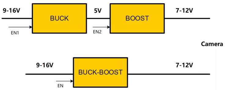
Figure 3: Power Supply Architecture Comparison
In a boost topology, even if we turn off the IC by pulling down EN, the output voltage (VOUT) is still equal to the input voltage (VIN). The subsequent load cannot be completely turned off unless additional switches are connected in series. Using a single-stage buck-boost solution such as the MPQ8873-AEC1 leads to high efficiency, saves layout area, and allows EN to be fully controlled for the output power supply.
Simple Layout
The MPQ8873-AEC1 provides a buck-boost topology with four integrated MOSFETs, which can dynamically adjust VOUT (see Figure 4).

Figure 4: Four Integrated MOSFETs for the MPQ8873
Besides the filter inductive capacitors and bootstrap (BST) capacitors, the peripheral circuit is straightforward and requires fewer components than traditional circuits.
High Efficiency
The MPQ8873-AEC1 integrates 10mΩ high-side MOSFETs (HS-FETs) and low-side MOSFETs (LS-FETs) and 25mΩ HS-FETs and LS-FETs. Under the test conditions of VIN = 13.5V, VOUT = 11.5V, and the load current (ILOAD) = 3A, the MPQ8873-AEC1’s efficiency exceeds 95% (see Figure 5).

Figure 5: MPQ8873 Efficiency Curve (VIN = 13.5V, VOUT = 11.5V, ILOAD = 3A)
Improved EMI
For convenience, the MPQ8873-AEC1’s layout allows designers to minimize the input and output power loops. The device also supports frequency spread spectrum (FSS), which further reduces EMI. Figure 6 shows the MPQ8873-AEC1’s minimal loop design.

Figure 6: MPQ8873 Minimal Loop Design
Versatile Car USB Connection Port Solution
The vehicle’s internal CPU generally accepts data from multiple USBs in different locations, including the armrest box or the front panel. The USB charging and data ports located in the hand-held box are equipped with USB charging ICs and a hub chip at the remote end. These ports cluster data to send to the CPU (see Figure 7). The USB port located on the front panel integrates the USB charging function into the car infotainment system, which can present new challenges to USB charging ICs.

Figure 7: Data Transmitted to CPU from Multiple USBs
The MPQ4228-C-AEC1 is a monolithic, step-down switch mode converter that can address the issues faced by USB charging ICs.
Excellent Versatility
The MPQ4228-C-AEC1 can be configured as USB-A or USB-C. Since the MPQ4228-C-AEC1 supports the USB BC1.2 CDP protocol, its charging port can provide about 10W to 15W of charging power while the phone and car interact with the USB output.

Figure 8: The MPQ4228-C Supports USB-A, USB-C, and CDC Protocols
More Detailed Considerations
In addition to the length of the mobile phone’s charging cable, the car and the front panel USB charging port are a certain distance apart. This means the actual voltage that reaches the mobile phone port may significantly differ from the vehicle's VOUT. The MPQ4228-C-AEC1 provides a line drop compensation function, which means that the higher the charging current, the higher the MPQ4228-C-AEC1’s VOUT. The line drop compensation slope can be designed with external resistance for flexibility and convenience.
Safe Protection
Accidents can occur when using the car charging port, such as plugging the mobile phone’s charging cable connector into the incorrect port. The MPQ4228-C-AEC1 provides short battery protection for I/O pins such as VBUS, DM, DP, and CC. This protection function prevents damage to the car charging IC (see Figure 9).
Improved Data Signal Chain Transmission
The eye diagram test evaluates the integrity of USB2.0 signals. Figure 9 shows that the MPQ4228-C-AEC1 demonstrates excellent eye diagram performance. In particular, the MPQ4228-C-AEC1 can pass the eye diagram test when the USB2.0 DMDP data passes through the device’s internal data switch using a 150cm cable.
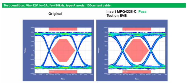
Figure 9: MPQ4228-C Passes the Eye Diagram Test
Improved EMI Performance
The MPQ4228-C-AEC1 provides a frequency spread spectrum (FSS) function to improve EMI, and its evaluation board can pass the national standard Grade 5 test without shielding and common-mode inductors (see Figure 10).

Figure 10: Improved EMI Performance for the MPQ4228-C
Comprehensive USB-IF Certification
The MPQ4228-C-AEC1 is certified by USB-IF. In particular, the device’s unique over-current protection (OCP) function enables the device to pass Apple’s MFI R33 certification test. When running an over-current transient pulse test (e.g. when the output experiences a short circuit), the MPQ4228-C-AEC1 maintains VBUS without shutting off during short-term over-current conditions (see Figure 11).
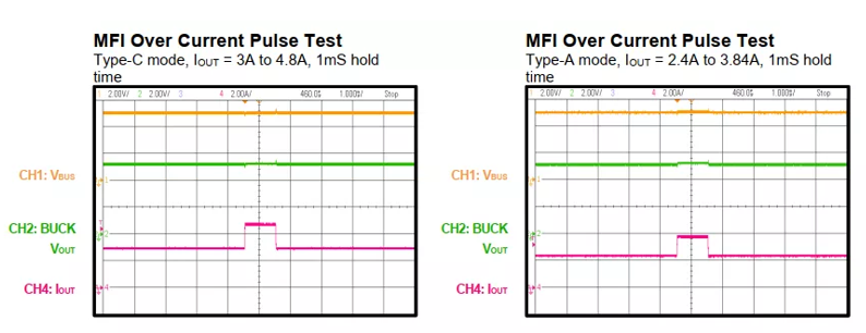
Figure 11: MPQ4228-C Maintains VBUS during Over-Current Loads
Conclusion
Following our review of primary and secondary power supplies in Part I, Part II proposed solutions for requirement challenges faced by camera power supplies and USB charging. The MPQ8873-AEC1 was used as a solution for surround-view camera modules, while the MPQ4228-C-AEC1 was used to mitigate USB charging challenges. MPS offers a robust and flexible portfolio of products that provide numerous advantages for the design of modern car infotainment systems.
_______________________
Did you find this interesting? Get valuable resources straight to your inbox - sent out once per month!
Technical Forum
 Latest activity 9 hours ago
 1 Comment
Latest activity 2 weeks ago
3 Comments
Latest activity 3 weeks ago
2 Comments
1 Comment
Latest activity 2 weeks ago
3 Comments
Latest activity 3 weeks ago
2 Comments
Log in to your account
Create New Account