Designing Multiple Independent Auxiliary Power Supplies with Magnetic Isolation

Get valuable resources straight to your inbox - sent out once per month
We value your privacy
Introduction
In a DC/DC converter, the auxiliary power supply of multiple switching devices requires independent isolated power supplies. Taking a full-bridge converter as an example, the high-side and low-side MOSFETs (HS-FETs and LS-FETs, respectively) of the bridge arm require isolated power supplies for the gate driver circuit. The traditional scheme uses a bootstrap circuit to power supply both the upper and lower devices with one independent power source. This solution is simple, reliable, and low-cost.
When multiple switch MOSFETs are connected in series in the bridge arm, multiple bootstrap circuits are required for the power supply, leading to challenges with cost. At the same time, in the bootstrap circuit, the supply voltage of the HS-FET is lower than that of the LS-FET, with a difference of a diode’s voltage drop. The on-state characteristics of the two MOSFETs are not completely symmetrical.
Figure 1 shows a switched-tank converter (STC), where an auxiliary power supply can be shared for the three LS-FETs on the right side, the three HS-FETs can be powered using the bootstrap circuit, and the corresponding auxiliary power supply is required for the four MOSFETs on the left side.
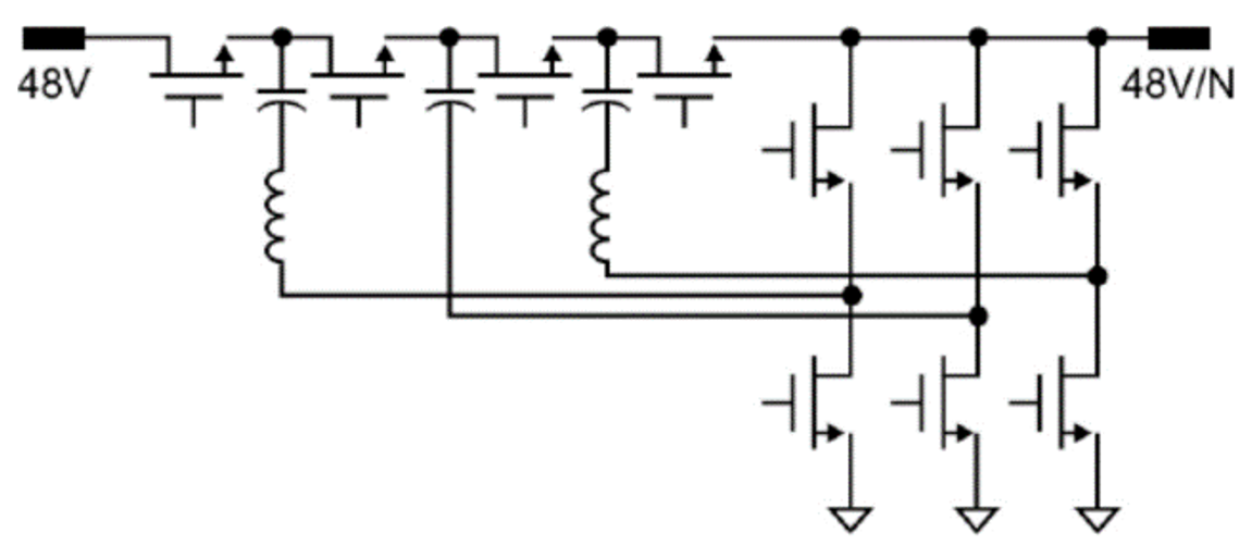
Figure 1: Switched-Tank Converter (STC)
Related Content
-
VIDEO
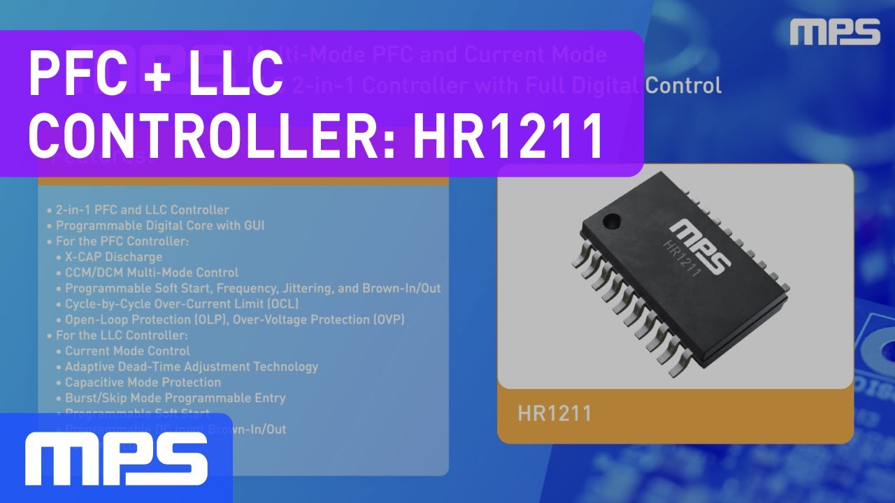
Multi-Mode PFC and Current Mode LLC 2-in-1 Controller: HR1211
The HR1211 is a multi-mode PFC and current mode LLC 2-in-1 controller with full digital control via a UART interface.
-
APPLICATION NOTE
Multi-Mode PFC + Current Mode LLC Controller
The HR1211 is a combination controller that integrates Multi-Mode PFC and Current Mode HB LLC controllers and exhibits very high performance.
-
USE CASE
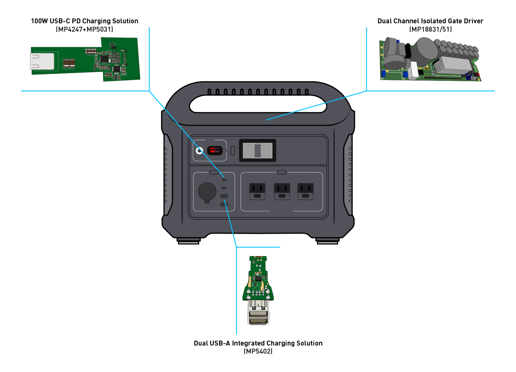
Isolated Gate Drivers Use Case: Portable Power Stations
MPS’s MP188xx family of isolated gate drivers help engineers create designs with integrated inverters that enable these batteries to charge directly from a wall outlet (AC to DC conversion), and also allows these batteries to be used to power small appliances directly (DC to AC conversion).
-
ARTICLE

DC Fast Charging System: Maximizing Power Density with an LLC Transformer Driver
As the world strives for carbon neutrality, electric vehicles (EVs) are rapidly taking market share from internal combustion engine vehicles.
Adopting a bootstrap circuit causes a certain voltage drop in each stage of the circuit, resulting in inconsistent conduction states for the device. Using multiple independent power supplies poses additional costs.
In a modular multilevel converter (MMC), many independent power supplies are required to supply power to the gate-level driver circuits due to the large number of modules. This raises issues with cost and complexity. MPS’s HR1211 is a multi-mode PFC and current mode LLC combo controller that can be applied to new auxiliary power supply methods to provide multi-channel, independent power supplies that are mutually isolated and reliable for power electronic converters.
A wireless power supply using an independent power supply at the transmitter can provide multiple independent auxiliary power supplies with magnetic isolation via multiple decoupled receiving coils. Figure 2 shows multiple independent auxiliary power supplies incorporating the HR1211, MP1907A MOSFET driver, and MPQ2029-AEC1 low-dropout (LDO) regulator. This design scheme uses wireless energy transmission systems to achieve multi-channel magnetic isolation.
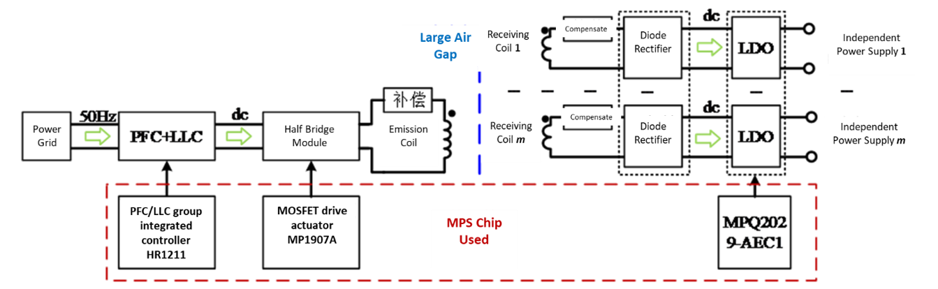
Figure 2: Multiple Independent Auxiliary Power Supplies with the HR1211, MP1907A, and MPQ2029-AEC1
Figure 3 shows the topology of an isolated independent auxiliary power wireless charging system. The parameters in this system are defined below (where x = 1, 2, 3, or 4):
- VINV is the inverter’s DC input voltage
- LT is the transmitting coil
- LF is the compensation inductor
- LRx is the receiving coil
- CT, CF, and CRx are the compensation capacitors
- Mx is the mutual inductance between the transmitting and receiving coils (LRx)
- VRECx is the DC output voltage of the of N-channel rectifier
- RLx is the N-channel load resistance.
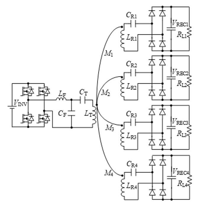
Figure 3: Quad-Receiver Wireless Charging System Topology
Figure 4 shows the coil structure model based on the finite element simulation software.
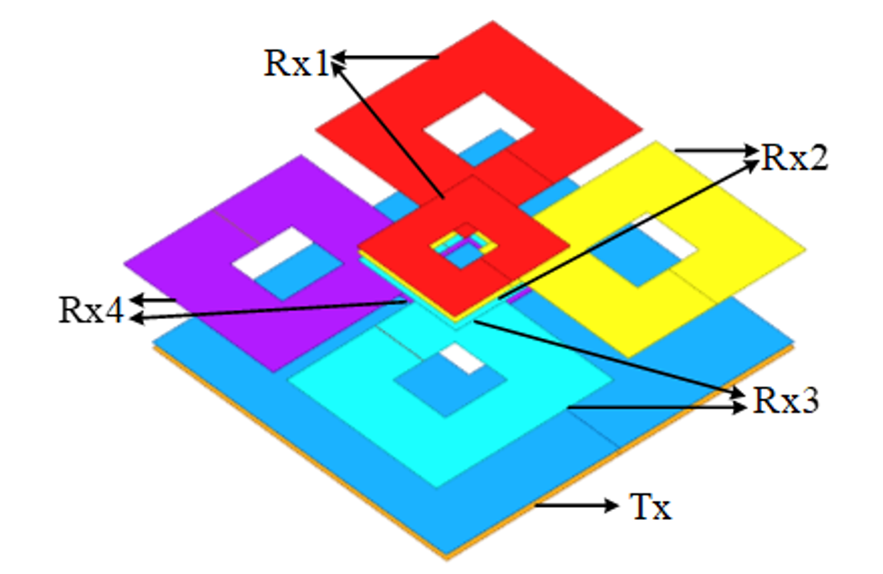
Figure 4: Coupling Mechanism Design
Figure 5 shows the corresponding PCB coils of the four receiving coils that are decoupled from each other.
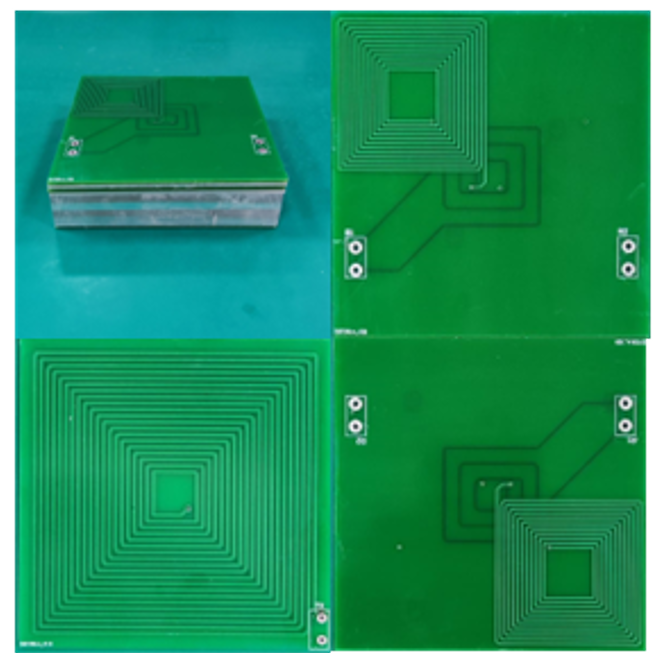
Figure 5: PCB Diagram of Transmitting and Receiving Coils
This scheme is simple, reliable, and meets the electrical isolation and insulation level requirements. MPS products can be widely applied to an auxiliary power supply design with multi-channel isolation across PFC and LCC combo controllers, inverter modules, and LDO regulators.
PFC and LLC Combo Controller
Power factor correction (PFC) converts alternating current (AC) from the power grid into direct current (DC). Energy is transferred from the transmitting side to the receiving side through the transmitting coil.
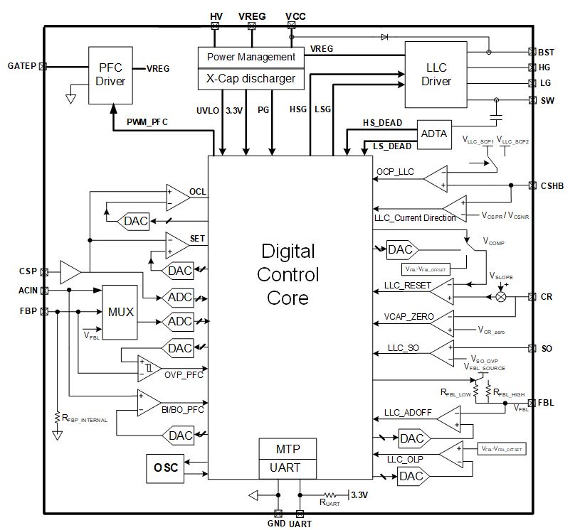
The HR1211 is configurable via the UART interface. Its integrated power-saving technology helps optimize efficiency over the full operating voltage range. The PFC controller employs a patented digital average current control scheme to enable mixed continuous conduction mode (CCM) and discontinuous conduction mode (DCM).
Under heavy loads, CCM reduces the peak current of the MOSFETs and extends the load range of the controller. Under light loads, DCM reduces the switching frequency for higher efficiency. Burst mode uses configurable, digital soft switching to improve light-load efficiency and reduce audible noise.
The LLC stage adopts current control mode to achieve excellent stability and fast response. Depending on the load conditions, there are three different operating modes that can be implemented: steady-state mode, frequency hopping mode, and burst mode. In this way, efficiency under different load conditions can be optimized separately. Under light loads, a frequency-controlled digital burst mode reduces switching power loss and audible noise. Additionally, adaptive dead-time adjustment (ADTA) and capacitive mode protection (CMP) ensure zero-voltage switching (ZVS) without requiring capacitive mode.
The HR1211 can be started up with an internal high-voltage (HV) current source. This eliminates the need for traditional start-up resistors or external circuitry. When the AC signal is lost, the HV current source functions as an X-capacitor discharger, eliminating the need for capacitive resistors. A variety of protections are provided, including thermal shutdown, PFC open-loop protection (OLP), over-voltage protection (OVP), over-current limit (OCL), LLC over-current protection (OCP), SO pin protection and over-power protection (OPP). Figure 6 shows the HR1211’s typical application circuit.
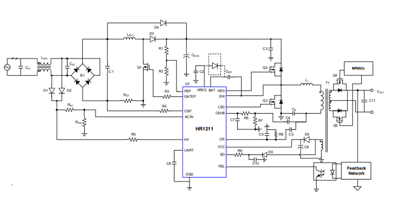
Figure 6: HR1211 Typical Application Circuit
Inverter Module
An inverter converts DC voltage into AC voltage, with a typical frequency of 85kHz. The MOSFETs must have sufficient withstand voltage and heat dissipation capability. The digital signal processor (DSP) generates the pulse-width modulation (PWM) signals to the driver circuit, which controls the switching of the MOSFETs. The MP1907A is a high-frequency, 100V, half-bridge, N-channel power MOSFET driver. Its low-side (LS) and high-side (HS) drive channels are independently controlled and matched with a time delay of less than 5ns. Under-voltage lockout (UVLO) protection for both the HS and LS drive voltages forces the outputs low in the event of insufficient power supply. Both outputs remain low until a rising edge on either input is detected. The integrated bootstrap diode reduces external component count. The MP1907A is available in a QFN-10 (3mmx3mm) package.
Figure 7 shows the MP1907A’s typical application circuit.
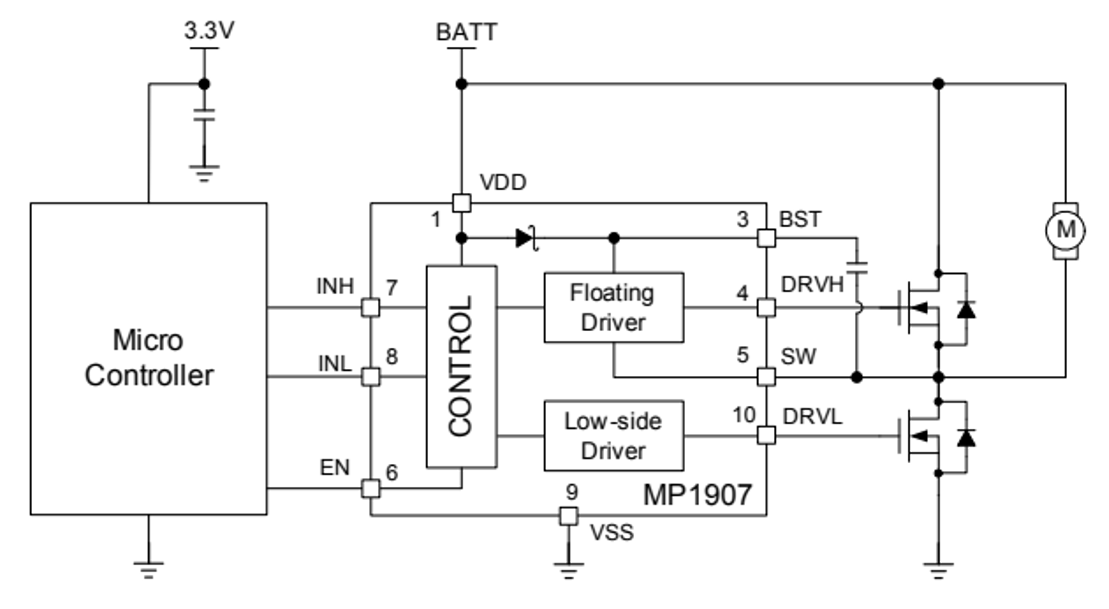
Figure 7: MP1907A Typical Application Circuit
Figure 8 shows the schematic diagram of the inverter circuit design.
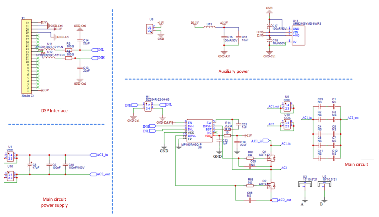
Figure 8: Schematic Diagram of the Inverter Circuit
Low-Dropout (LDO) Regulator
An LDO regulator is a DC step-down linear regulator that maintains a stable output voltage (VOUT) even when the input voltage (VIN) or load current changes. Modern LDO circuits feature small size, low noise, low power consumption, low price, and ease of use.
The MPQ2029-AEC1 is a low-power linear regulator that uses high-voltage batteries to supply power to systems. The device offers a 3V to 40V VIN range, LDO voltage, and low quiescent supply current. The low quiescent current and low dropout voltage allows for operation at extremely low power levels, making the MPQ2029-AEC1 ideal for low-power microcontrollers and battery-operated equipment.
The MPQ2029-AEC1 provides an adjustable VOUT range between 1.25V and 15V. The regulator's output current is limited internally, and the device is protected against short-circuit, overload, and over-temperature conditions. The MPQ2029-AEC1 is available in an SOIC-8EP package.
Figure 9 shows the MPQ2029-AEC1’s typical application circuit.
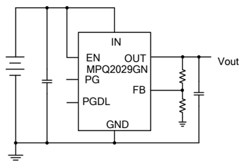
Figure 9: MPQ2029 Typical Application Circuit
Conclusion
This article explored designing multiple independent auxiliary power supplies and wireless power transmission systems to achieve a multi-channel, magnetically isolated, independent auxiliary power supply scheme using the HR1211, MP1907A, and MPQ2029-AEC1. Compared to traditional schemes that use a bootstrap circuit to power the auxiliary power supply, using an independent power supply provides the advantages of being simple, reliable, and low-cost.
For more details, explore MPS’s broader selection of PFC/LLC controllers, MOSFET drivers, and LDOs.
_______________________
Did you find this interesting? Get valuable resources straight to your inbox - sent out once per month!
Technical Forum
 Latest activity 4 hours ago
 1 Comment
Latest activity 12 hours ago
1 Comment
Latest activity 12 hours ago
5 Comments
1 Comment
Latest activity 12 hours ago
1 Comment
Latest activity 12 hours ago
5 Comments
Log in to your account
Create New Account